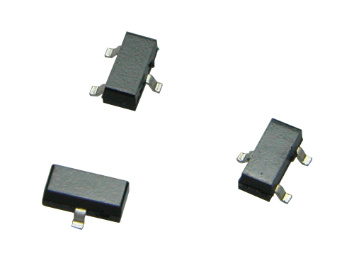
PinoutDescriptionBipolar transistors, also called junction type transistors, are a kind of transistors. Unlike field-effect transistors (unipolar transistors), they are called bipolar because they have two kinds of carriers (hole, electron) The SBT5401 is designed as one kind of PNP silicon trans...
SBT5401: PinoutDescriptionBipolar transistors, also called junction type transistors, are a kind of transistors. Unlike field-effect transistors (unipolar transistors), they are called bipolar because they h...
SeekIC Buyer Protection PLUS - newly updated for 2013!
268 Transactions
All payment methods are secure and covered by SeekIC Buyer Protection PLUS.

The SBT5401 is designed as one kind of PNP silicon transitors which would be the general purpose amplifier and for the high voltage application.
SBT5401 has three features. (1)High collector breakdown voltage :Vcbo=-160V, Vceo=-150V. (2)Low collector saturation voltage: Vce(sat)=-0.5V(max). (3)Complementary pair with SBT5551. Those are all the main features.
Some absolute maximum ratings of SBT5401 have been concluded into several points as follow. (1)Its collector to base voltage would be -160V. (2)Its collector to emitter voltage would be -150V. (3)Its emitter to base voltage would be -5V. (4)Its collector current would be -600mA. (5)Its collector dissipation would be 200mW. (6)Its junction temperature would be 150°C. (7)Its storage temperature range would be from -55°C to 150°C. It should be noted that stresses above those listed in absolute maximum ratings may cause permanent damage to device.
Also some electrical characteristics of SBT5401 are concluded as follow. (1)Its collector to base breakdown voltage would be min -160V. (2)Its collector to emitter breakdown voltage would be min -150V. (3)Its emitter to base breakdown voltage would be min -5V. (4)Its collector cut-off current would be max -100nA. (5)Its emitter cut-off current would be max -100nA. (6)Its DC current gain would be min 50 with condition of Vce=-5V, Ic=-1mA and would be min 60 and max 240 with conditions of Vce=-5V and Ic=-10mA and would be min 50 with conditions of Vce=-5V, Ic=-50mA. (7)Its collector to emitter saturation voltage would be max -0.2V with conditions of Ic=-10mA and Ib=-1mA and would be max -0.5V with conditions of Ic=-50mA, Ib=-5mA. (8)Its base to emitter saturation voltage would be max -1V. (9)Its transition frequency would be min 100MHz and max 400MHz. (10)Its collector output capacitance would be max 6pF. And so on. At present we have not got so much information about this IC and we would try hard to get more information about it. If you have any question or suggestion or want to know more information please contact us for details. Thank you!