Features: 1.5 Gbps per channel
Low power: 70 mA in dual repeater mode @1.5 Gbps
Low output jitter
Configurable 0/25/50/100% pre-emphasis drives lossy backplanes and cables
Non-blocking architecture allows 1:2 splitter, 2:1 mux, crossover, and dual buffer configurations
Flow-through pinout
LVDS/BLVDS/CML/LVPECL inputs, LVDS Outputs
IEEE 1149.1 and 1149.6 compliant
Single 3.3V supply
Separate control of inputs and outputs allows for power savings
Industrial -40 to +85°C temperature range
28-lead LLP package, or 32-lead LQFP package
Pinout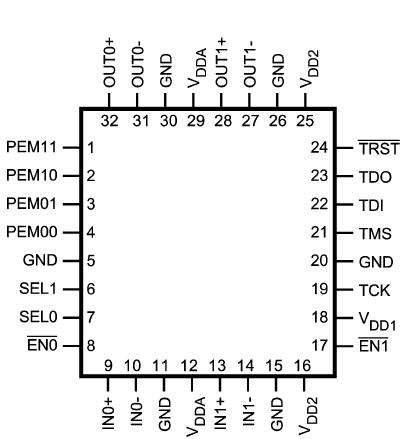 Specifications
If Military/Aerospace specified devices are required, please contact the National Semiconductor Sales Office/Distributors for availability and specifications.
Supply Voltage(VDD) -0.3Vto+4V
GMOS/LVTTL Input Voltage -0.3V to (VDD +0.3V)
LVDS Receiver Input Voltage -0.3V to +3.6V
LVDS Driver Output Voltage -0.3V to +3.6V
LVDS Output Short Circuit 40mA
Junction Temperature +150°C
Storage Temperature -65°C to +150°C
Lead Temperature (Soldering, 4 sec) +260°C
Maximum Package Power Dissipation Capacity @ 25°C
LLp-28 4.31W
LQFP-32 1.47W
Derating above 25°C
LLP-28 34.5 mW/°C
LQFP-32 11.8 mW/°C
Thermal Resistance, JA
LLP-28 29°C/W
LQFP-32 85°C/W
ESD Rating
HBM, 1.5 k, 100 pF 6.5 kV
EIAJ, 0, 200 pF >250V
Description
The SCAN90CP02 is a 1.5 Gbps 2 x 2 LVDS crosspoint switch. High speed data paths and flow-through pinout minimize internal device jitter, while configurable 0/25/50/100% pre-emphasis overcomes external ISI jitter effects of lossy backplanes and cables. The differential inputs interface to LVDS and Bus LVDS signals such as those on National's 10-, 16-, and 18- bit Bus LVDS SerDes, as well as CML and LVPECL. The SCAN90CP02 can also be used with ASICs and FPGAs. The non-blocking crosspoint architecture is pinconfigurable as a 1:2 clock or data splitter, 2:1 redundancy mux, crossover function, or dual buffer for signal booster and stub hider applications.
Integrated IEEE 1149.1 (JTAG) and 1149.6 circuitry supports testability of both single-ended LVTTL/CMOS and differential LVDS PCB interconnect. The 3.3V supply, CMOS process, and LVDS I/O ensure high performance at low power over the entire industrial -40 to +85°C temperature range.

 SCAN90CP02 Data Sheet