Features: · Word-organized, reprogrammable nonvolatile memory in
n-channel floating-gate technology (E2PROM)
· 1024 ´ 8-bit organization
· Supply voltage 5 V
· Serial 2-line bus for data input and output (I2C Bus)
· Reprogramming mode, 10 ms erase / write cycle
· Reprogramming by means of on-chip control
(without external control)
· The end of the programming cycle can be checked
· Data retention in excess of 10 years
· More than 104 reprogramming cycles per addressPinout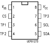 Specifications
| Parameter |
Symbol |
Limit Values |
Unit |
| min. |
max. |
| Supply voltage |
VCC |
0.3 |
6 |
V |
| Input voltage |
VI |
0.3 |
6 |
V |
| Power dissipation |
PD |
|
130 |
mW |
| Storage temperature |
Tstg |
40 |
125 |
°C |
| Thermal resistance (system-air) |
R th SA |
|
100 |
K/W |
| Junction temperature |
Tj |
|
85 |
°C |
| Supply voltage |
VCC |
4.75 |
5.25 |
V |
| Ambient temperatureAmbient temperature |
TA |
0 |
70 |
°C |
DescriptionI
2C Bus Interface
The I
2C Bus SDA 2586-5 is a bidirectional 2-line bus for the transfer of data between various integrated circuits. SDA 2586-5 consists of a data line SDA and a clock line SCL. The data line require an external pull-up resistor to V
CC (open drain output stages).
The possible operational states of the I
2C Bus SDA 2586-5 are shown in figure 1. In the quiescent state, both lines SDA and SCL are high, i.e. the output stages are disabled. As long as SCL remains "1", information changes on the data bus indicate the start or the end of a data transfer between two components. The transition on SDA from "1" to "0" is a start condition, the transition from "0" to "1" a stop condition. During a data transfer, the information about SDA 2586-5 on the data bus will only change when the clock line SCL is "0". The information on SDA is valid as long as SCL is "1".
In conjunction with an I
2C Bus system, the SDA 2586-5 can operate as a receiver, and as a transmitter (slave receiver/listener, or slave transmitter/talker). Between a start and a stop condition, the information is always transmitted in byte-organized form. Between the falling edge of the eighth transmission pulse and a ninth acknowledge clock pulse, the device sets the SDA-line to low as a reception confirmation, if the SDA 2586-5 select conditions have been met. During the output of data, the data output of the memory SDA 2586-5 becomes high in impedance during the ninth clock pulse (acknowledge master).
The signal timing required for the operation of the I2C Bus SDA 2586-5 is summarized in figure 2.

 SDA 2586-5 Data Sheet


