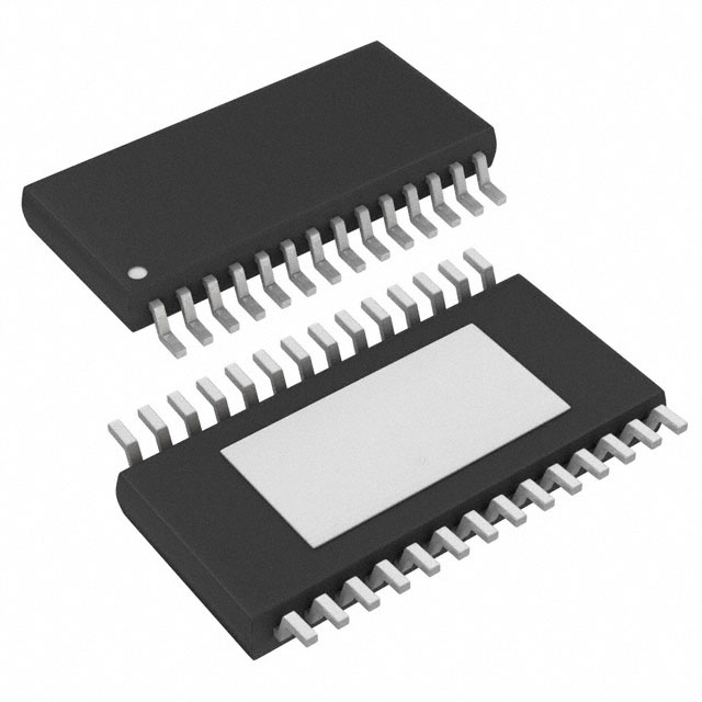
Features: • Low input power range 0 to 6 dBm• High efficiency- GSM850 49%- GSM900 53%- DCS 53%- PCS 53%• Internal ICC sense resistor for PAC• Closed loop iPAC or open loop operation with external PAC circuit• Input/Output matching 50 Ω internal (with DC blocking...
SKY77324: Features: • Low input power range 0 to 6 dBm• High efficiency- GSM850 49%- GSM900 53%- DCS 53%- PCS 53%• Internal ICC sense resistor for PAC• Closed loop iPAC or open loop op...
SeekIC Buyer Protection PLUS - newly updated for 2013!
268 Transactions
All payment methods are secure and covered by SeekIC Buyer Protection PLUS.
US $2.23 - 3.32 / Piece
Clock Synthesizer / Jitter Cleaner 2.1GHz 100Hz step Freq. Synthesizer
US $2.05 - 2.48 / Piece
Clock Synthesizer / Jitter Cleaner 2.1GHz 100Hz step Freq. Synthesizer
| Parameter |
Minimum |
Maximum |
Unit |
| Input Power (PIN) |
- |
15 |
dBm |
| Supply Voltage (VCC), Standby, VAPC 0.3 V, PAC ENABLE 0.2 V |
- |
7 |
V |
| Control Voltage (VAPC) |
0.5 |
VCC_MAX 0.2 (See Table 3) |
V |
| Storage Temperature |
55 |
+100 |
°C |
The SKY77324 Power Amplifier Module (PAM) is designed in a low profile (1.2 mm), compact form factor for quad-band cellular handsets comprising GSM850/900, DCS1800, and PCS1900 operation. The PAM also supports Class 12 General Packet Radio Service (GPRS) multi-slot operation.
The module SKY77324 consists of separate GSM850/900 PA and DCS1800/PCS1900 PA blocks, impedance-matching circuitry for 50 Ω input and output impedances, and a Power Amplifier Control (PAC) block with an internal current-sense resistor. The custom CMOS integrated circuit provides the internal PAC function and interface circuitry. Fabricated onto a single Gallium Arsenide (GaAs) die, one Heterojunction Bipolar Transistor (HBT) PA block of SKY77324 supports the GSM850/900 bands and the other supports the DCS1800 and PCS1900 bands. Both PA blocks share common power supply pins to distribute current. The GaAs die, the Silicon (Si) die, and the passive components are mounted on a multi-layer laminate substrate. The assembly of SKY77324 is encapsulated with plastic overmold.
RF input and output ports of the SKY77324 are internally matched to a 50 Ω load to reduce the number of external components for a quad-band design. Extremely low leakage current (2.5 µA, typical) of the dual PA module maximizes handset standby time. The SKY77324 also contains band-select switching circuitry to select GSM (logic 0) or DCS/PCS (logic 1) as determined from the Band Select (BS) signal. In Figure 1, below, the BS pin selects the PA output (DCS/PCS OUT or GSM850/900 OUT) and the Analog Power Control (VAPC) controls the level of output power.
VBATT and VSENSE pins of SKY77324 connect to an internal current-sense resistor and interface to an integrated power amplifier control (iPAC™) function, which is insensitive to variations in temperature, power supply, and process. The PAC NABLE input allows initial turn-on of PAC circuitry to minimize battery drain.