SpecificationsHigh efficiency:45% (GSM900)40% (DCS1800)Current limiting for protection and extended battery lifeInput/Output internally matched 50 TXVCO-to-antenna and antenna-to-RX-SAW filter RF interfaceTX harmonics below 36 dBmSmall, low profile package7 mm x 6 mm x 0.9 mm30-pad configurationLo...
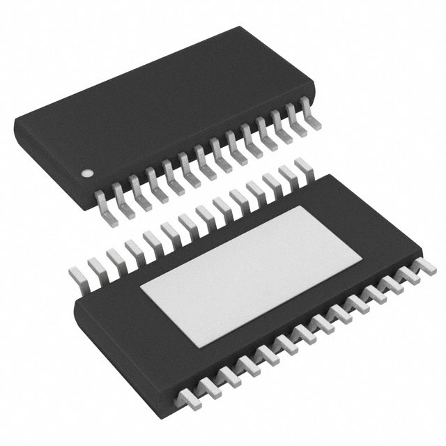
SKY77546: SpecificationsHigh efficiency:45% (GSM900)40% (DCS1800)Current limiting for protection and extended battery lifeInput/Output internally matched 50 TXVCO-to-antenna and antenna-to-RX-SAW filter RF in...
SeekIC Buyer Protection PLUS - newly updated for 2013!
268 Transactions
All payment methods are secure and covered by SeekIC Buyer Protection PLUS.
US $2.23 - 3.32 / Piece
Clock Synthesizer / Jitter Cleaner 2.1GHz 100Hz step Freq. Synthesizer
US $2.05 - 2.48 / Piece
Clock Synthesizer / Jitter Cleaner 2.1GHz 100Hz step Freq. Synthesizer
The SKY77546 is a transmit and receive Front-End Module (FEM) designed in a compact form factorfor dual-band cellular handsets comprising GSM900 and DCS1800 operation. The SKY77546 offers acomplete Transmit VCO-to-Antenna and Antenna-to-Receive SAW filter solution that supports Class12 General Packet Radio Service (GPRS) multi-slot operation and EDGE operation for handsets andmodules.
The module SKY77546 consists of a GSM900 PA block and a DCS1800 PA block, impedance-matching circuitryfor 50 input and output impedances, TX harmonics filtering, high linearity and low insertion loss RFswitches, and a Power Amplifier Control (PAC) block. A custom CMOS integrated circuit provides theinternal PAC function, external interface circuitry, and decoder circuitry to control the RF switches.The integrated PAC function provides envelope amplitude control by reducing sensitivity to input drive,temperature, power supply, and process variations. The Heterojunction Bipolar Transistor (HBT) PA blocks of SKY77546 are fabricated onto a single InGaP/GaAs die. One PA block supports the GSM900 band and theother PA block supports the DCS1800 band. Both PA blocks share common power supply pads todistribute current. The output of each PA block and the outputs to the two receive pads are connectedto the antenna pad through a diplexer and SP2T switch. The GaAs die, switch die, Silicon (Si) die, andpassive components are mounted on a multi-layer laminate substrate. The assembly of SKY77546 is encapsulatedwith plastic overmold.
Band selection and control of transmit and receive RF signal flows of SKY77546 are performed using five externalcontrol pads. The band select pad (BS) selects GSM or DCS modes of operation. The TxEN pad selectsreceive or transmit mode of the respective RF switch (Tx = logic 1). SW_EN provides improvedisolation for flexibility in control timing to meet the required time mask. MODE configures theamplifier for GMSK operation (MODE = 0) or linear EDGE operation (MODE = 1). Proper timing of thelogic on these pads, and Analog Power Control (APC) of SKY77546 allows for high isolation between the antennaand Tx-VCO while the VCO is being tuned prior to the transmit burst. Standby mode provides a lowcurrentconsumption state. Low leakage current (6.5 A, typical) of the dual PA module maximizeshandset standby time.