Features: ·Working voltage: 3.0V ~ 3.6V For L Version
4.5V ~ 5.5V For C Version
·General 8052 family compatible
·12 clocks per machine cycle
·64K byte on chip program flash
·1024 byte on-chip data RAM
·Three 16 bit Timers/Counters
·One Watch Dog Timer
·Four 8-bit I/O ports for PDIP package
·Four 8-bit I/O ports + one 4-bit I/O ports for PLCC or QFP package
·Full duplex serial channel
·Bit operation instruction
·Industrial Level
·8-bit Unsigned Division
·8-bit Unsigned Multiply
·BCD arithmetic
·Direct Addressing
·Indirect Addressing
·Nested Interrupt
·Two priority level interrupt
·A serial I/O port
·Power save modes: Idle mode and Power down mode
·Code protection function
·Low EMI (inhibit ALE)
·Bank mapping direct addressing mode for access on-chip RAM
·5 channel SPWM function with P1.3 ~ P1.7Pinout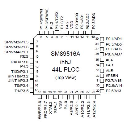 Description
The SM89516A series product is an 8 - bit single chip micro controller with 64KB on-chip flash and 1K byte RAM embedded. It is a derivative of the 8052 micro controller family. It has 5-channel SPWM build-in. User can access on-chip expanded RAM with easier and faster way by its bank mapping direct addressing mode' scheme. With its hardware features and powerful instruction set, it's straight forward to make it a versatile and cost effective controller for those applications which demand up to 32 I/ O pins for PDIP package or up to 36 I/O pins for PLCC/QFP package, or applications which need up to 64K byte flash memory for program data. To program the on-chip flash memory, a commercial writer is available to do it in parallel programming method.
The SM89516A is designed as one kind of 8-bit single chip micro controller with 64KB flash & 1KB RAM embedded that belongs to the SM89516 family. Features of this device are:(1)64K byte on chip program flash; (2)1024 bytes data RAM; (3)three 16 bit Timers/Counters; (4)four 8-bit I/O ports for PDIP package; (5)four 8-bit I/O ports + one 4-bit I/O ports for PLCC or QFP package; (6)full duplex serial channel; (7)bit operation instruction; (8)page free jumps; (9)8-bit unsigned division; (10)8-bit unsigned multiply; (11)BCD arithmetic operation; (12)direct addressing; (13)indirect addressing; (14)nested interrupt; (15)two priority level interrupts; (16)a serial I/O port; (17)power save modes: idle mode and power down mode; (18)code protection function; (19)one watch dog timer (WDT); (20)low EMI (inhibit ALE).
The absolute maximum ratings of the SM89516A can be summarized as:(1)Operating temperature: 0 to 70 ;(2)Supply voltage: 4.5 to 5.5 V;(3)Oscillator Frequency: 3.0 to 16 MHz;(4)Input Low Voltage (port 0,1,2,3,4,#EA): -0.5 to 0.8 V;(5)Input High Voltage (port 0,1,2,3,4,#EA): 2.0 to Vcc+0.5 V;(6)Output Low Voltage: 0.45 V;(7)Logical 0 Input Current: -75 uA;(8)Logical Transition Current: -650 uA;(9)Input Leakage Current: ±10 uA. If you want to know more information about the SM89516A, please download the datasheet in www.seekic.com or www.chinaicmart.com .

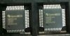
 SM89516A Data Sheet