Features: ` Highest-Performance Fixed-Point Digital Signal Processors (DSPs)
− 2-, 1.67-, 1.39-ns Instruction Cycle Time
− 600-MHz Clock Rate
− Eight 32-Bit Instructions/Cycle
− Twenty-Eight Operations/Cycle
− 4800 MIPS
− Fully Software-Compatible With C62x
− C6414/15/16 Devices Pin-Compatible
` VelociTI.2TMExtensions to VelociTITM Advanced Very-Long-Instruction-Word (VLIW) TMS320C64xTM DSP Core
− Eight Highly Independent Functional Units With VelociTI.2TM Extensions:
− Six ALUs (32-/40-Bit), Each Supports Single 32-Bit, Dual 16-Bit, or Quad 8-Bit Arithmetic per Clock Cycle
− Two Multipliers Support Four 16 x 16-Bit Multiplies (32-Bit Results) per Clock Cycle or Eight 8 x 8-Bit Multiplies (16-Bit Results) per Clock Cycle
− Non-Aligned Load-Store Architecture
− 64 32-Bit General-Purpose Registers
− Instruction Packing Reduces Code Size
− All Instructions Conditional
` Instruction Set Features
− Byte-Addressable (8-/16-/32-/64-Bit Data)
− 8-Bit Overflow Protection
− Bit-Field Extract, Set, Clear
− Normalization, Saturation, Bit-Counting
− VelociTI.2TMIncreased Orthogonality
` Viterbi Decoder Coprocessor (VCP) [C6416]
− Supports Over 500 7.95-Kbps AMR
− Programmable Code Parameters
` Turbo Decoder Coprocessor (TCP) [C6416]
− Supports up to Six 2-Mbps 3GPP (6 Iterations)
− Programmable Turbo Code and Decoding Parameters
` L1/L2 Memory Architecture
− 128K-Bit (16K-Byte) L1P Program Cache (Direct Mapped)
− 128K-Bit (16K-Byte) L1D Data Cache (2-Way Set-Associative)
− 8M-Bit (1024K-Byte) L2 Unified Mapped RAM/Cache (Flexible Allocation)
` Two External Memory Interfaces (EMIFs)
− One 64-Bit (EMIFA), One 16-Bit (EMIFB)
− Glueless Interface to Asynchronous Memories (SRAM and EPROM) and Synchronous Memories (SDRAM,SBSRAM, ZBT SRAM, and FIFO)
− 1280M-Byte Total Addressable External Memory Space
` Enhanced Direct-Memory-Access (EDMA) Controller (64 Independent Channels)
` Host-Port Interface (HPI)
− User-Configurable Bus Width (32-/16-Bit)
` 32-Bit/33-MHz, 3.3-V PCI Master/Slave Interface Conforms to PCI Specification 2.2 [C6415/C6416 ]
− Three PCI Bus Address Registers:Prefetchable Memory Non-Prefetchable Memory I/O
− Four-Wire Serial EEPROM Interface
− PCI Interrupt Request Under DSP Program Control
− DSP Interrupt Via PCI I/O Cycle
` Three Multichannel Buffered Serial Ports
− Direct Interface to T1/E1, MVIP, SCSA Framers
− Up to 256 Channels Each
− ST-Bus-Switching-, AC97-Compatible
− Serial Peripheral Interface (SPI) Compatible (Motorola)
` Three 32-Bit General-Purpose Timers
` Universal Test and Operations PHY Interface for ATM (UTOPIA) [C6415/C6416]
− UTOPIA Level 2 Slave ATM Controller
− 8-Bit Transmit and Receive Operations up to 50 MHz per Direction
− User-Defined Cell Format up to 64 Bytes
` Sixteen General-Purpose I/O (GPIO) Pins
` Flexible PLL Clock Generator
` IEEE-1149.1 (JTAG†) Boundary-Scan-Compatible
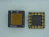
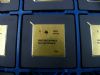
` 570-Pin Grid Array (PGA) Package (GAD Suffix)
` 0.13-m/6-Level Cu Metal Process (CMOS)
` 3.3-V I/Os, 1.4-V Internal
Application·Audio
·Automotive
·Broadband
·Digital Control
·Military
·Optical Networking
·Security
·Telephony
·Video & Imaging
·WirelessSpecificationsSupply voltage ranges: CVDD (see Note 1) . . . . . . . . . . . . . . . . . . . . − 0.3 V to 1.8 V
DVDD (see Note 1) . . . . . . . . . . . . . . . . . . . . . . −0.3 V to 4 V
Input voltage ranges: (except PCI), VI . . . . . . . . . . . . . . . . . . . . . . . . . . −0.3 V to 4 V
(PCI), VIP [C6415 and C6416 only] . . . .−0.5 V to DVDD + 0.5 V
Output voltage ranges: (except PCI), VO . . . . . . . . . . . . . . . . . . . . . . . . −0.3 V to 4 V
(PCI), VOP [C6415 and C6416 only] . .−0.5 V to DVDD + 0.5 V
Operating case temperature ranges, TC: . . . . . . . . . . . . . . . . . . . . . . .−55to 115
Storage temperature range, Tstg . . . . . . . . . . . . . . . . . . . . . . . . . . . . . .−65 to 150
† Stresses beyond those listed under "absolute maximum ratings" may cause permanent damage to the device. These are stress ratings only, and functional operation of the device at these or any other conditions beyond those indicated under "recommended operating conditions" is not implied. Exposure to absolute-maximum-rated conditions for extended periods may affect device reliability.
NOTE 1: All voltage values are with respect to VSS.
DescriptionThe TMS320C64xTM DSPs (including the SMJ320C6414, SMJ320C6415, and SMJ320C6416 devices) are the highest-performance fixed-point DSP generation in the TMS320C6000TMDSP platform. The TMS320C64xTM(C64xTM†) device is based on the second-generation high-performance, advanced VelociTITM very-long-instruction-word (VLIW) architecture (VelociTI.2TM) developed by Texas Instruments (TI), making these DSPs an excellent choice for multichannel and multifunctional applications. The C64xTM is a code-compatible member of the C6000 DSP platform.
With SMJ320C6416 performance of up to 5760 million instructions per second (MIPS) at a clock rate of 720 MHz, the C64x devices offer cost-effective solutions to high-performance DSP programming challenges. The C64x DSPs possess the operational flexibility of high-speed controllers and the numerical capability of array processors.The C64xTM DSP core processor has 64 general-purpose registers of 32-bit word length and eight highly independent functional units-two multipliers for a 32-bit result and six arithmetic logic units (ALUs)- with VelociTI.2TMextensions. The VelociTI.2TM extensions in the eight functional units include new instructions to accelerate the performance in key applications and extend the parallelism of the VelociTI architecture. The C64x can produce four 32-bit multiply-accumulates (MACs) per cycle for a total of 2400 million MACs per second (MMACS), or eight 8-bit MACs per cycle for a total of 4800 MMACS. The C64x DSP also has application-specific hardware logic, on-chip memory, and additional on-chip peripherals similar to the other C6000 DSP platform devices.
The C6416 device has two high-performance embedded coprocessors [Viterbi Decoder Coprocessor (VCP) and Turbo Decoder Coprocessor (TCP)] that significantly speed up channel-decoding operations on-chip. The VCP operating at CPU clock divided-by-4 can decode over 500 7.95-Kbps adaptive multi-rate (AMR) [K = 9,R = 1/3] voice channels. The VCP supports constraint lengths K = 5, 6, 7, 8, and 9, rates R = 1/2, 1/3, and 1/4,and flexible polynomials, while generating hard decisions or soft decisions. The TCP operating at CPU clock divided-by-2 can decode up to thirty-six 384-Kbps or six 2-Mbps turbo encoded channels (assuming 6 iterations). The TCP implements the max*log-map algorithm and is designed to support all polynomials and rates required by Third-Generation Partnership Projects (3GPP and 3GPP2), with fully programmable frame length and turbo interleaver. Decoding parameters such as the number of iterations and stopping criteria are also programmable. Communications between the VCP/TCP and the CPU are carried out through the EDMA controller.
The C64x uses a two-level cache-based architecture and has a powerful and diverse set of peripherals. The Level 1 program cache (L1P) is a 128K-bit direct mapped cache and the Level 1 data cache (L1D) is a 128K-bit 2-way set-associative cache. The Level 2 memory/cache (L2) consists of an 8M-bit memory space that is shared between program and data space. L2 memory can be configured as mapped memory or combinations of cache (up to 256K bytes) and mapped memory. The peripheral set includes three multichannel buffered serial ports (McBSPs); an 8-bit Universal Test and Operations PHY Interface for Asynchronous Transfer Mode (ATM) Slave [UTOPIA Slave] port (C6415/C6416 only); three 32-bit general-purpose timers; a user-configurable 16-bit or 32-bit host-port interface (HPI16/HPI32); a peripheral component interconnect (PCI) [C6415/C6416 only];a general-purpose input/output port (GPIO) with 16 GPIO pins; and two glueless external memory interfaces (64-bit EMIFA and 16-bit EMIFB‡), both of which are capable of interfacing to synchronous and asynchronous memories and peripherals.
The C64x has a complete set of development tools which includes: an advanced C compiler with C64x-specific enhancements, an assembly optimizer to simplify programming and scheduling, and a Windows debugger interface for visibility into source code execution.
TMS320C6000, C64x, and C6000 are trademarks of Texas Instruments.
Windows is a registered trademark of the Microsoft Corporation.
All trademarks are the property of their respective owners.
† Throughout the remainder of this document, the SMJ320C6414, SMJ320C6415, and SMJ320C6416 shall be referred to as SMJ320C64x or C64x where generic, and where specific, their individual full device part numbers will be used or abbreviated as C6414, C6415, or C6416.
‡ These C64xTM devices have two EMIFs (64-bit EMIFA and 16-bit EMIFB). The prefix "A" in front of a signal name indicates it is an EMIFA signal whereas a prefix "B" in front of a signal name indicates it is an EMIFB signal. Throughout the rest of this document, in generic EMIF areas of discussion, the prefix "A" or "B" may be omitted from the signal name.

 SMJ320C6416 Data Sheet