ApplicationFor the 'MCM42C, the location of the local memory has changed from that of the 'MCM42D. In addition, to make proper use of the local memory, it is necessary to understand how it is controlled.
In the case of the 'MCM42C, the lower 128K of memory is controlled by LSTRB0, while the upper 128K of memory is controlled by LSTRB1. Since the upper 128K begins at address 1000000h, it is necessary to load the value 10111 (binary) into the STRB ACTIVE area (bits 2824) of the local memory interface control register (LMICR). This process ensures that the 'C40 uses LSTRB0 to control the lower 128K and LSTRB1 to control the upper 128K.
In the case of the 'MCM42D, LSTRB0 controls the entire 128K. The value loaded into the STRB ACTIVE area of the LMICR after reset is sufficient to control the memory. This value is 1110, and tells the 'C40 that the entire local memory is controlled by LSTRB0.
This subject is discussed in depth in Chapter 9 of the 1996 TMS320C4x User's Guide (literature number SPRU063). In particular, section 9.3 discusses the proper use of the memory interface control registers.
SpecificationsSupply voltage range, VCC (see Note 1) . . . . . . . . . . . . . . . . . . . . . . . . . . . . . . . . . . . . . . 0.3 V to 7 V
Voltage range on any terminal . . . . . . . . . . . . . . . . . . . . . . . . . . . . . . . . . . . . . . . . . . . . . 0.3 V to 7 V
Output voltage range, VO . . . . . . . . . . . . . . . . . . . . . . . . . . . . . . . . . . . . . ... . . . . . . . . . . 0.3 V to 7 V
Operating free-air temperature range (commercial [L version]), TA . . . . . . . . . . . . . . . . . . 0°C to 70°C
(military [M version]), TA . . . . . . . . . . . . . . . . . . 55°C to 125°C
Junction temperature, TJ . . . . . . . . . . . . . . . . . . . . . . . . . . . . . . . . . . . . . . . . . . . . . . . . . . . . . . . . 150°C
Storage temperature range, Tstg . . . . . . . . . . . . . . . . . . . . . . . . . . . . . . . . . . . . . . . . . 65°C to 150°C
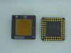
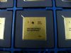
DescriptionThe '42 dual 'C40 multichip module (MCM) contains two SMJ320C40 digital signal processors (DSPs) with 128K words * 32 bits ('42D) or 256K words * 32 bits ('42C) of zero-wait-state SRAMs mapped to each local bus. Global address and data buses with two sets of control signals are routed externally for each processor, allowing external memory to be accessed. The external global bus provides a continuous address reach of 2G words.
The dual 'C40 configuration allows standard microprocessor initialization using the bootstrap loader. Both reset-vector-control terminals are brought out to external terminals for each processor. A single CLKIN line and a RESET line feed both processors in parallel, minimizing clock skew and allowing easy synchronization for interlocked operations.
Communication port 0 of CPU #1 connects to communication port 3 of CPU #2 for direct processor-to-processor communication.
The IEEE-1149.1 (JTAG) test ports of the 'C40s are connected serially to allow scan operations and emulation of the module as a whole. Testability of the '42 adds value and reduces development and support costs. Texas Instruments (TIE) offers a wide variety of ANSI/IEEE-1149.1 products and support.
The '42 dual 'C40 MCM is packaged in a 408-pin ceramic quad flat pack. The '42 dual 'C40 MCM is available
in both a commercial temperature range (0°C to 70°C) and a military temperature range (55°C to 125°C)
option.

 SMJ320MCM42D Data Sheet