ApplicationAudio
Automotive
Broadband
Digital Control
Military
Optical Networking
Security
Telephony
Video & Imaging
WirelessPinout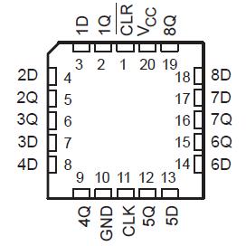 Specifications
Supply voltage range, VCC . . . . . . . . . . . . . . . . . . . . . . . . . . . . . . . . . . . . . . . . . . . . . . . . . . . . . .. . 0.5 V to 7 V
Input voltage range, VI (see Note 1) . . . . . . . . . . . . . . . . . . . . . . . . . . . . . . . . . . . . . . . . . . . . . . . . . . 0.5 V to 7 V
Voltage range applied to any output in the high or power-off state, VO . . . . . . . . . . . . . . . . . . . 0.5 V to 5.5 V
Current into any output in the low state, IO: SN54ABT273 . . . . . . . . . . . . . . . . . . . . . . . . . . . . . . . . . . . . 96 mA
SN74ABT273 . . . . . . . . . . . . . . . . . . . . . . . . . . . . . . . . . . . 128 mA
Input clamp current, IIK (VI < 0) . . . . . . . . . . . . . . . . . . . . . . . . . . . . . . . . . . . . . . . . . . . . . . . . . . . . . . . . . . 18 mA
Output clamp current, IOK (VO < 0) . . . . . . . . . . . . . . . . . . . . . . . . . . . . . . . . . . . . . . . . . . . . . . . . . . . . . . . 50 mA
Package thermal impedance, JA (see Note 2): DB package . . . . . . . . . . . . . . . . . . . . . . . . . . . . . . . . 115°C/W
DW package . . . . . . . . . . . . . . . . . . . . . . . . . . . . . . . . . 97°C/W
N package . . . . . . . . . . . . . . . . . . . . . . . . . . . . . . . . . . . 67°C/W
PW package . . . . . . . . . . . . . . . . . . . . . . . . . . . . . . . . 128°C/W
Storage temperature range, Tstg . . . . . . . . . . . . . . . . . . . . . . . . . . . . . . . . . . . . . . . . . . . . . . . . . . . 65°C to 150°C
DescriptionThe SN54ABT273 are 8-bit positive-edge-triggered D-type flip-flops with a direct clear (CLR) input. SN54ABT273 are particularly suitable for implementing buffer and storage registers, shift registers, and pattern generators.
Information at the data (D) inputs meeting the setup time requirements is transferred to the Q outputs on the positive-going edge of the clock pulse. Clock triggering occurs at a particular voltage level and is not directly related to the transition time of the positive-going pulse. When the clock (CLK) input is at either the high or low level, the D input signal has no effect at the output. The SN54ABT273 is characterized for operation over the full military temperature range of 55°C to 125°C. The
SN74ABT273 is characterized for operation from 40°C to 85°C.

 SN54ABT273 Data Sheet


