Features: ` State-of-the-Art EPIC-IIBTM BiCMOS Design Significantly Reduces Power Dissipation
` Latch-Up Performance Exceeds 500 mA Per JEDEC Standard JESD-17
` Typical VOLP (Output Ground Bounce) < 1 V at VCC = 5 V, TA = 25°C
` High-Drive Outputs (32-mA IOH, 64-mA IOL)
` Package Options Include Plastic Small-Outline (DW), Shrink Small-Outline (DB), and Thin Shrink Small-Outline (PW) Packages, Ceramic Chip Carriers (FK), Ceramic Flat (W) Package, and Plastic (N) and Ceramic (J) DIPs
Pinout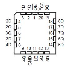 Specifications
Supply voltage range, VCC . . . . . . . . . . . . . . . . . . . . . . .. . . . . . . . . . . . . . . . . . . 0.5 V to 7 V
Input voltage range, VI (see Note 1) . . . . . . . . . . . . . . . . . . . . . . . . . . . . . . . . . 0.5 V to 7 V
Voltage range applied to any output in the high or power-off state, VO . . . . . 0.5 V to 5.5 V
Current into any output in the low state, IO: SN54ABT373 . . . . . . . . . . . . . . . . . . . . . . . 96 mA
SN74ABT373 . . . . . . . . . . . . . . . . . . . . . . 128 mA
Input clamp current, IIK (VI < 0) . . . . . . . . . . . . . . . . . . . . . . . . . . . . . . . . . . . . . . . . . . 18 mA
Output clamp current, IOK (VO < 0) . . . . . . . . . . . .. . . . . . . . . . . . . . . . . . . . . . . . . . . . 50 mA
Package thermal impedance, qJA (see Note 2): DB package . . . . . . . . . .. . . . . . . . . . 115°C/W
DW package . . . . . . . . . . . . . . . . . . . . 97°C/W
N package . . . . . . . . . . . . . . . . . . . . . . 67°C/W
PW package . . . . . . . . . . . . . . . . . . . . 128°C/W
Storage temperature range, Tstg . . . . . . . . . . . . . . . . . . . . . . . . . . . . . . . . . . 65°C to 150°C
‡ Stresses beyond those listed under "absolute maximum ratings" may cause permanent damage to the device. These are stress ratings only, and functional operation of the device at these or any other conditions beyond those indicated under "recommended operating conditions" is not implied. Exposure to absolute-maximum-rated conditions for extended periods may affect device reliability.
NOTES: 1. The input and output negative-voltage ratings may be exceeded if the input and output clamp-current ratings are observed.
2. The package thermal impedance is calculated in accordance with EIA/JEDEC Std JESD51, except for through-hole packages, which use a trace length of zero.
DescriptionThe eight latches of the 'ABT373 are transparent D-type latches. While the latch-enable (LE) input is high, the Q outputs follow the data (D) inputs. When LE is taken low, the Q outputs of SN54ABT373 are latched at the logic levels set up at the D inputs.
A buffered output-enable (OE) input of SN54ABT373 can be used to place the eight outputs in either a normal logic state (high or low logic levels) or a high-impedance state. In the high-impedance state, the outputs of SN54ABT373 neither load nor drive the bus lines significantly. The high-impedance state and increased drive provide the capability to drive bus lines without need for interface or pullup components.
OE does not affect the internal operations of the latches. Old data of SN54ABT373 can be retained or new data can be entered while the outputs are in the high-impedance state.
To ensure the high-impedance state during power up or power down, OE should be tied to VCC through a pullup resistor; the minimum value of the resistor SN54ABT373 is determined by the current-sinking capability of the driver.
The SN54ABT373 is characterized for operation over the full military temperature range of 55°C to 125°C. The SN74ABT373 is characterized for operation from 40°C to 85°C.

 SN54ABT373 Data Sheet


