SN54ABT827

Features: State-of-the-Art EPIC-II BTM BiCMOS Design Significantly Reduces Power DissipationFlow-Through Architecture Optimizes PCB LayoutLatch-Up Performance Exceeds 500 mA Per JEDEC Standard JESD-17Typical VOLP (Output Ground Bounce) < 1 V at VCC = 5 V, TA = 25°C High-Impedance State During P...

product image

SN54ABT827 Picture
SeekIC No. : 004496366 Detail

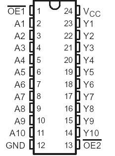
SN54ABT827: Features: State-of-the-Art EPIC-II BTM BiCMOS Design Significantly Reduces Power DissipationFlow-Through Architecture Optimizes PCB LayoutLatch-Up Performance Exceeds 500 mA Per JEDEC Standard JESD-...

floor Price/Ceiling Price

Part Number:
SN54ABT827
Supply Ability:
5000

Price Break

  • Qty
  • 1~5000
  • Unit Price
  • Negotiable
  • Processing time
  • 15 Days
Total Cost: $ 0.00

SeekIC Buyer Protection PLUS - newly updated for 2013!

  • Escrow Protection.
  • Guaranteed refunds.
  • Secure payments.
  • Learn more >>

Month Sales

268 Transactions

Rating

evaluate  (4.8 stars)

Upload time: 2025/12/24

Payment Methods

All payment methods are secure and covered by SeekIC Buyer Protection PLUS.

Notice: When you place an order, your payment is made to SeekIC and not to your seller. SeekIC only pays the seller after confirming you have received your order. We will also never share your payment details with your seller.
Product Details

Description


Features:

 State-of-the-Art EPIC-II BTM BiCMOS Design Significantly Reduces Power Dissipation
 Flow-Through Architecture Optimizes PCB Layout
 Latch-Up Performance Exceeds 500 mA Per JEDEC Standard JESD-17
 Typical VOLP (Output Ground Bounce) < 1 V at VCC = 5 V, TA = 25°C
High-Impedance State During Power Up and Power Down
 High-Drive Outputs (32-mA IOH, 64-mA IOL)
 Package Options Include Plastic Small-Outline (DW), Shrink Small-Outline (DB), and Thin Shrink Small-Outline (PW) Packages, Ceramic Chip Carriers (FK), and Plastic (NT) and Ceramic (JT) DIPs


Pinout

  Connection Diagram


Specifications

Supply voltage range, VCC . . . . . . . . . . . . . . . . . . . . . . . . . . . . . . . . . . . . . . .  . . . . . . . 0.5 V to 7 V
Input voltage range,  VI(see Note 1) . . . . . . .  . . . . .  . . . . . . . . . . . . .. . .. . . . . . . . . . .0.5 V to 7 V
Voltage applied to any output in the high state or power-off state, VO  . . .  . . . . .  . .0.5 V to 5.5 V
Current into any output in the low state, IO: SN54ABT827 . . . . . . . . . . . . .. . . . . . . . . . . . .. . .96 mA 
                                                                       SN74ABT827  . . . . . . . . . . . . . . . . . . . . . . . ..   .128 mA
Input clamp current, IIK (VI < 0) . . . . . . . . . . . . . . . . . . . . . . . . . . . . . . . .. . . . . . . . . . . . . . .. .18 mA
Output clamp current, IOK (VO < 0)  . . . . . . . . . . . . . . . . . . . . . . . . . . . . . . . . . . . . . . . . . . . . .50 mA
Package thermal impedance, JA (see Note 2): DB package  . . . .  . . . .  . . . . . . . . . . . .   . . .104°C/W
                                                                          DW package  . . . .. . . . .   . . . . . . . . . . . . . . . .81°C/W
                                                                          NT package  . . . .. . . . . . . .  . . . . .. . . . . . .  . . 67°C/W
                                                                          PW package  . . . . . . . . . .  . . . . . . . . . . . . .. .120°C/W
Storage temperature range, Tstg . . . . . . . . . . . . . . . . . . . . . . . . . . . . . . . . .    . . .. . . .65°C to 150°C


Description

These 10-bit buffers or bus drivers of SN54ABT827 provide a high-performance bus interface for wide data paths or buses carrying parity.

The 3-state control gate is a 2-input AND gate with active-low inputs so that if either output-enable (OE1 or OE2) input is high, all ten outputs are in the high-impedance state. The SN54ABT827 provide true data at the outputs.

When VCC is between 0 and 2.1 V, the SN54ABT827 is in the high-impedance state during power up or power down. However, to ensure the high-impedance state above 2.1 V, OE should be tied to VCC through a pullup resistor; the minimum value of the resistor SN54ABT827 is determined by the current-sinking capability of the driver.

The SN54ABT827 is characterized for operation over the full military temperature range of 55°C to 125°C. The SN74ABT827 is characterized for operation from 40°C to 85°C.


Customers Who Bought This Item Also Bought

Margin,quality,low-cost products with low minimum orders. Secure your online payments with SeekIC Buyer Protection.
Crystals and Oscillators
Cables, Wires
Circuit Protection
Cables, Wires - Management
Isolators
View more