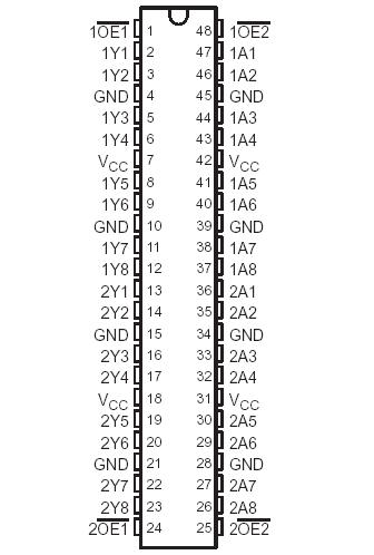
Features: Members of the Texas InstrumentsWidebusTMFamilyEPICETM(Enhanced-Performance ImplantedCMOS) ProcessInputs Are TTL-Voltage CompatibleDistributed VCC and GND Pins MinimizeHigh-Speed Switching NoiseFlow-Through Architecture Optimizes PCBLayoutLatch-Up Performance Exceeds 250 mA PerJESD 17ESD...
SN54AHCT16540: Features: Members of the Texas InstrumentsWidebusTMFamilyEPICETM(Enhanced-Performance ImplantedCMOS) ProcessInputs Are TTL-Voltage CompatibleDistributed VCC and GND Pins MinimizeHigh-Speed Switching...
SeekIC Buyer Protection PLUS - newly updated for 2013!
268 Transactions
All payment methods are secure and covered by SeekIC Buyer Protection PLUS.
Features: PinoutSpecificationsDescriptionThe SN54/74LS147 and SN54/74LS148 are Priority Encoders. ...
PinoutDescriptionThe LS155 and LS156 are Dual 1-of-4 Decoder/Demultiplexers with common Address in...

Supply voltage range,VCC . . . . . . . . . . . . . . . . . . . . . . . . . . .. . . . .. . . . . . . . . . . 0.5 V to 7 V
Input voltage range, VI (see Note 1) . . . . . . . . . . . . . . . . . . . . . . . . . . . . . . . . . .0.5 V to 7 V
Output voltage range, VO (see Note 1) . . . . . . . . . . . . . . . . . . . . .. . . .0.5 V to VCC + 0.5 V
Input clamp current, IIK (VI < 0) . . . . . . . . . . . . . . . . . . . . . . . . . . . . . . . . . .. . . . . . . .20 mA
Output clamp current, IOK (VO < 0 or VO > VCC) . .. . . . . . . . . . . . . . . . . . . . . . . . . . . . .±20 mA
Continuous output current, IO (VO = 0 to VCC) . . . . . . . . . . . . . . . .. . . . . . . . . . . . . . .±25 mA
Continuous current through each VCC or GND . . . . . . . . . . . . . . . . . . . . . . . . . . . . . . . .±75 mA
Package thermal impedance, qJA (see Note 2): DGG package . . . . . . . . . . . .. . . . . . . . .70/W
DGV package . . . .. . . . . . . . . . . . . . . . .58°C/W
DL package . . . . . . . . . . . . . . . . . . . .. .63°C/W
Storage temperature range, Tstg . . . . . . . . . . . . . . . . . . . . . . . . . . . . . . . . . . . . . 65 to 150
These 16-bit buffers and bus drivers SN54AHCT16540 provide ahigh-performance bus interface for wide datapaths.
The 3-state control gate is a 2-input AND gate withactive-low inputs so that if either output-enable(OE1 or OE2) input is high, all correspondingoutputs are in the high-impedance state.
To ensure the high-impedance state during power up or power down, OE should be tied to VCC through a pullup resistor; the minimum value of the resistor SN54AHCT16540 is determined by the current-sinking capability of the driver.
The SN54AHCT16540 is characterized for operation over the full military temperature range of 55°C to 125°C.
The SN74AHCT16540 is characterized for operation from 40°C to 85°C.