Features: • State-of-the-Art BiCMOS Design Significantly Reduces ICCZ
• Full Parallel Access for Loading
• Buffered Control Inputs
• 3-State Bus-Driving Inverted Outputs
• ESD Protection Exceeds 2000 V Per MIL-STD-883C, Method 3015
• Package Options Include Plastic Small-Outline (DW) Packages, Ceramic Chip Carriers (FK) and Flatpacks (W), and Plastic and Ceramic 300-mil DIPs (J, N)
Pinout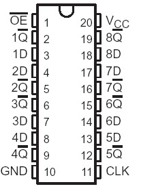 Specifications
Supply voltage range, VCC . . . . . . . . . . . . . . . . . . . . . . . . . . . . . . . . . . . . . . . . . . . . . . .. . . 0.5 V to 7 V
Input voltage range, VI (see Note 1) . . . . . . . . . . . . . . . . . . . . . . . . . . . . . . . . . . . . . . . . . . 0.5 V to 7 V
Voltage range applied to any output in the disabled or power-off state, VO . . . . . . . . . . 0.5 V to 5.5 V
Voltage range applied to any output in the high state, VO . . . . . . . . . . . . . . . . . . . .. . . . . . 0.5 V to VCC
Input clamp current . . . . . . . . . . . . . . . . . . . . . . . . . . . . . . . . . . . . . . . . . . . . . . . . . . . . . . . . . . . . .30 mA
Current into any output in the low state: SN54BCT534 . . . . . . . . . . . . . . . . . . . . . . . . . . . . . . . . . .96 mA
SN74BCT534 . . . . . . . . . . . . . . . . . . . . . . . . . . . . . . . . . .128 mA
Operating free-air temperature range: SN54BCT534 . . . . . . . . . . . . . . . . . . . . . . . . . . . 55°C to 125°C
SN74BCT534 . . . . . . . . . . . . . . . . . . . . . . . . . . . . . .0°C to 70°C
Storage temperature range . . . . . . . . . . . . . . . . . . . . . . . . . . . . . . . . . . . . . . . . . . . . . . . . 65°C to 150°C
DescriptionThe SN54BCT534 is an 8-bit flip-flop with 3-state outputs designed specifically for driving highly capacitive or relatively low-impedance loads. SN54BCT534 is particularly suitable for implementing buffer registers, I/O ports, bidirectional bus drivers, and working registers.
The eight flip-flops of the 4BCT534 are edge-triggered D-type flip-flops. On the positive transition of the clock, the Q outputs will be set to the complement of the logic levels that were set up at the data (D) inputs. The 4BCT534 provides inverted data at its outputs.
A buffered output-enable (OE) input of SN54BCT534 can be used to place the eight outputs in either a normal logic state (high or low logic levels) or a high-impedance state. In the high-impedance state, the outputs of SN54BCT534 neither load nor drive the bus lines significantly. The high-impedance state and the increased drive provide the capability to drive bus lines without need for interface or pullup components.
The output-enable (OE) input does not affect the internal operations of the flip-flop. Previously stored data of SN54BCT534 can be retained or new data can be entered while the outputs are in the high-impedance state.
The SN54BCT534 is characterized for operation over the full military temperature range of 55°C to 125°C. The SN74BCT534 is characterized for operation from 0°C to 70°C.

 SN54BCT534 Data Sheet


