Features: Members of the Texas Instruments WidebusTM Family
Universal Bus Transceiver (UBTTM) Combines D-Type Latches and D-Type Flip-Flops for Operation in Transparent,Latched, Clocked, or Clock-Enabled Mode
GTL Buffered CLKAB Signal (CLKOUT)
Translate Between GTL/GTL+ Signal Level and LVTTL Logic Levels
Support Mixed-Mode (3.3 V and 5 V) Signal Operation on A-Port and Control Inputs
Equivalent to '16601 Function
Ioff Supports Partial-Power-Down Mode Operation
Bus Hold on Data Inputs Eliminates th Need for External Pullup/Pulldown Resistors on A Port
Latch-Up Performance Exceeds 100 mA Per JESD 78, Class II
Distributed VCC and GND-Pin Configuration Minimizes High-Speed Switching Noise
Package Options Include Plastic Shrink Small-Outline (DL), Thin Shrink Small-Outline (DGG), and Ceramic Flat (WD) PackagesPinout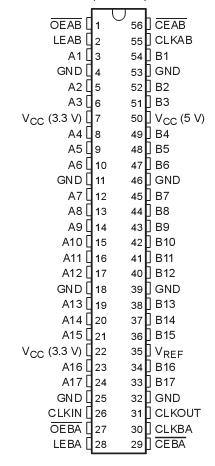 Specificationsabsolute maximum ratings over operating free-air temperature range (unless otherwise noted)
Supply voltage range, VCC: 3.3 V . . . . . . . . . . . . . . . . . . . . . . . . . . . . . . . . . . . . . 0.5 V to 4.6 V
5 V . . . . . . . . . . . . . . . . . . . . . . . . . . . . . . . . . . . . . . 0.5 V to 7 V
Input voltage range, VI (see Note 1): A-port and control inputs . . . . . . . . . . . . . . . 0.5 V to 7 V
B port and VREF . . . . . . . . . . . . . . . . . . . 0.5 V to 4.6 V
Voltage range applied to any output in the high or power-off state, VO
(see Note 1): A port . . . . . . . . . . . . . . . . . . . . . . . . . . . . . . . . . . . . . . . . . . . . . . . . 0.5 V to 7 V
B port . . . . . . . . . . . . . . . . . . . . . . . . . . . . . . . . . . . . . . . . . . . . .. . . 0.5 V to 4.6 V
Current into any output in the low state, IO : A port . . . . . . . . . . . . . . . . . . . . . . . . . . . . . 128 mA
B port . . . . . . . . . . . . . . . . . . . . . . . . . . . . . . 80 mA
Current into any A-port output in the high state, IO (see Note 2) . . . . . . . . . . . . . . . . . . . . 64 mA
Continuous current through each VCC or GND . . . . . . . . . . . . . . . . . . . . . . . . . . . . . . . . . . 100 mA
Input clamp current, IIK (VI < 0) . . . . . . . . . . . . . . . . . . . . . . . . . . . . . . . . . . . . . . . . . . . . 50 mA
Output clamp current, IOK (VO < 0) . . . . . . . . . . . . . . . . . . . . . . . . . . . . . . . . . . . . . . . . . 50 mA
Package thermal impedance, q JA (see Note 3): DGG package . . . . . . . . . . . . . . . . . . . . . 64°C/W
DL package . . . . . . . . . . . . . . . . . . . . . . . . . . . . . . . . . . . . . . . . . . . . . . . . . . . . . . . . . . . 56°C/W
Storage temperature range, Tstg . . . . . . . . . . . . . . . . . . . . . . . . . . . . . . . . . . . .. 65°C to 150°C
Description The SN54GTL16616 is 17-bit universal bus transceivers (UBTs) that provide LVTTL-to-GTL/GTL+ and GTL/GTL+-to-LVTTL signal-level translation. They combine D-type flip-flops and D-type latches to allow for transparent, latched, clocked, and clocked-enabled modes of data transfer identical to the '16601 function. Additionally, they provide for a copy of CLKAB at GTL/GTL+ signal levels (CLKOUT) and conversion of a GTL/GTL+ clock to LVTTL logic levels (CLKIN). The SN54GTL16616 provides an interface between cards operating at LVTTL logic levels and a backplane operating at GTL/GTL+ signal levels.Higher-speed operation is a direct result of the reduced output swing (<1 V), reduced input threshold levels, and output edge control (OEC
TM).
The user has the flexibility of using SN54GTL16616 at either GTL (V
TT = 1.2 V and V
REF= 0.8 V) or the preferred higher noise margin GTL+ (V
TT = 1.5 V and V
REF = 1 V) signal levels. GTL+ is the Texas Instruments derivative of the Gunning transceiver logic (GTL) JEDEC standard JESD 8-3. The B port normally operates at GTL or GTL+ signal levels, while the A-port and control inputs are compatible with LVTTL logic levels and are 5-V tolerant. V
REF is the reference input voltage for the B port. V
CC (5 V) supplies the internal and GTL circuitry while V
CC (3.3 V) supplies the LVTTL output buffers.

 SN54GTL16616 Data Sheet


