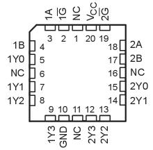
Pinout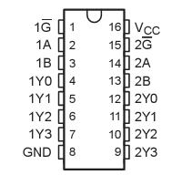
 Specifications
Supply voltage range, VCC. . . . . . . . . . . . . . . . . . . . . . . . . . . . . . . . . . . . . . . . . . . . . . . .-0.5 V to 7 V
Input clamp current, IIK (VI < 0 or VI > VCC ) (see Note 1) . . . . . . . . . . . . . . . . . . . . . . . . . ±20 mA
Output clamp current, IOK (VO < 0 or V O > VCC ) (see Note 1) . . . . . . . . . . . . . . . . . . . . ±20 mA
Continuous output current, IO (VO = 0 to VCC ) . . . . . . . . . . . . . . . . . . . . . . . . . . . . . . . . . ±25 mA
Continuous current through VCC or GND . . . . . . . . . . . . . . . . . . . . . . . . . . . . . . . . . . . . . . ±50 mA
Package thermal impedance, JA (see Note 2): D package . . . . . . . . . . . . . . . . . . . . . . . . . . .73/W
DB package . . . . . . . . . . . . . . . . . . . . . . . . . . . . . . . . ............................................................ 82/W
N package . . . . . . . . . . . . . . . . . . . . . . . . . . . . . . . . . . .......................................................... 67/W
NS package . . . . . . . . . . . . . . . . . . . . . . . . . . . . . . . ...............................................................64/W
PW package . . . . . . . . . . . . . . . . . . . . . . . . . . . . . . ............................................................. 108/W
Storage temperature range, Tstg . . . . . . . . . . . . . . . . . . . . . . . . . . . . . . . . . . . . . . . . .-65to 150
+Stresses beyond those listed under "absolute maximum ratings" may cause permanent damage to the device. These are stress ratings only, and functional operation of the device at these or any other conditions beyond those indicated under "recommended operating conditions" is not implied. Exposure to absolute-maximum-rated conditions for extended periods may affect device reliability.
NOTES: 1. The input and output voltage ratings may be exceeded if the input and output current ratings are observed.
2. The package thermal impedance is calculated in accordance with JESD 51-7.
DescriptionThe SN54HC139 is designed for high-performance memory-decoding or data-routing applications requiring very short propagation delay times. In high-performance memory systems, these decoders can minimize the effects of system decoding. When employed with high-speed memories utilizing a fast enable circuit, the delay time of these decoders and the enable time of the memory usually are less than the typical access time of the memory. This means that the effective system delay introduced by the decoders is negligible.

 SN54HC139 Data Sheet


