Features: 3-State Version of 'HC151
Wide Operating Voltage Range of 2 V to 6 V
High-Current 3-State Outputs Interface Directly With System Bus or Can Drive Up To 15 LSTTL Loads
Low Power Consumption, 80-A Max ICC
Typical tpd = 9 ns
±6-mA Output Drive at 5 V
Low Input Current of 1 A Max
Perform Parallel-to-Serial Conversion
Complementary Outputs Provide True and Inverted DataPinout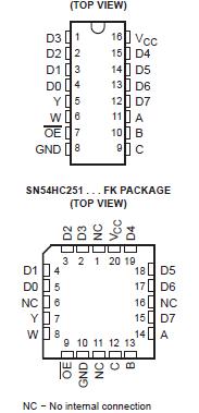 Specifications
Supply voltage range, VCC . . . . . . . . . . . . . . . . . . . . . . . . . . . . . . . . . . . . . −0.5 V to 7 V
Input clamp current, IIK (VI < 0 or VI > VCC) (see Note 1) . . . . . . . . . . . . . . . . .±20 mA
Output clamp current, IOK (VO < 0 or VO > VCC) (see Note 1) . . . . . . . . . . . . . . ±20 mA
Continuous output current, IO (VO = 0 to VCC) . . . . . . . . . . . . . . . . . . . . . . . . . ±35 mA
Continuous current through VCC or GND . . . . . . . . . . . . . . . . . . . . . . . . . . . . . ..±70 mA
Package thermal impedance, JA (see Note 2): D package . . . . . . . . . . . . . . .. 73/W
DB package . . . . . . . . . . . . . . ... 82/W
N package . . . . . . . . . . . . .. . . 67/W
NS package . . . . . . . . . . . . . . . . 64/W
PW package . . . . . . . . . . . . . .. 108/W
Storage temperature range, Tstg . . . . . . . . . . . . . . . . . . . . . . . . . . . . . . ..−65 to 150
† Stresses beyond those listed under "absolute maximum ratings" may cause permanent damage to the device. These are stress ratings only,and
functional operation of the device at these or any other conditions beyond those indicated under "recommended operating conditions" is not implied. Exposure to absolute-maximum-rated conditions for extended periods may affect device reliability.
NOTES: 1. The input and output voltage ratings may be exceeded if the input and output current ratings are observed.
2. The package thermal impedance is calculated in accordance with JESD 51-7.
DescriptionThese data selectors/multiplexers contain full binary decoding to select 1-of-8 data sources and feature strobe-controlled complementary 3-state
outputs.
The 3-state outputs of SN54HC251 can interface with and drive data lines of bus-organized systems. With all but one of the common outputs disabled (in the
high-impedance state), the low impedance of the single enabled output drives the bus line to a high or low logic level. Both outputs of SN54HC251 are controlled by the output-enable (OE) input. The outputs are disabled when OE is high.

 SN54HC251 Data Sheet


