Features: ` Inputs Are TTL-Voltage Compatible
` Contain Eight D-Type Flip-Flops
` Direct Clear Input
` Applications Include:
Buffer/Storage Registers
Shift Registers
Pattern Generators
` Package Options Include Plastic Small-Outline (DW) and Ceramic Flat (W) Packages, Ceramic Chip Carriers (FK), and Standard Plastic (N) and Ceramic (J) 300-mil DIPs
Pinout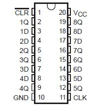 Specifications
Supply voltage range, VCC . . . . . . . . . . . . . . . . . . . . . . . . . . . . . . . . . . . . . . 0.5 V to 7 V
Input clamp current, IIK (VI < 0 or VI > VCC) (see Note 1) . . . . . . . . . . . . . . . . . . . ±20 mA
Output clamp current, IOK (VO < 0 or VO > VCC) (see Note 1) . . . . . . . . . .. . . . . . . ±20 mA
Continuous output current, IO (VO = 0 to VCC) . . . . . . . . . . . . . . . . . . . . . . . . . . . . ±25 mA
Continuous current through VCC or GND . . . . . . . . . . . . . . . . . . . . . . . . . . . . . . . . . ±50 mA
Package thermal impedance, JA (see Note 2): DW package . . . . . . . . . . . . . . . . . 97°C/W
N package . . . . . . . . . . . . . . . . . . 67°C/W
PW package . . . . . . . . . . . . . . . . 128°C/W
Storage temperature range, Tstg . . . . . . . . . . . . . . . . . . . . . . . . . . . . . . . 65°C to 150°C
† Stresses beyond those listed under "absolute maximum ratings" may cause permanent damage to the device. These are stress ratings only, and functional operation of the device at these or any other conditions beyond those indicated under "recommended operating conditions" is not implied. Exposure to absolute-maximum-rated conditions for extended periods may affect device reliability.
NOTES: 1. The input and output voltage ratings may be exceeded if the input and output current ratings are observed.
2. The package thermal impedance is calculated in accordance with JESD 51, except for through-hole packages, which use a trace length of zero.
DescriptionSN54HCT273 is positive-edge-triggered D-type flip-flops with a common enable input. The 'HCT273 are similar to the 'HCT377, but feature a common clear enable (CLR) input instead of a latched clock.
Information at the data (D) inputs of SN54HCT273 meeting the setup time requirements is transferred to the Q outputs on the positive-going edge of the clock (CLK) pulse. Clock triggering occurs at a particular voltage level and is not directly related to the positive-going pulse. When CLK is at either the high or low level, the D input has no effect at the output. The circuits of SN54HCT273 are designed to prevent false clocking by transitions at CLR.
The SN54HCT273 is characterized for operation over the full military temperature range of 55°C to 125°C. The SN74HCT273 is characterized for operation from 40°C to 85°C.

 SN54HCT273 Data Sheet


