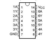
Features: *Convert TTL Voltage Levels to MOS Levels*High Sink-Current Capability*Input Clamping Diodes Simplify System Design*Open-Collector Driver for Indicator Lamps and Relays*Inputs Fully Compatible With Most TTL CircuitsPinoutSpecificationsSupply voltage, VCC . . . . . . . . . . . . . . . . ....
SN54LS06: Features: *Convert TTL Voltage Levels to MOS Levels*High Sink-Current Capability*Input Clamping Diodes Simplify System Design*Open-Collector Driver for Indicator Lamps and Relays*Inputs Fully Compat...
SeekIC Buyer Protection PLUS - newly updated for 2013!
268 Transactions
All payment methods are secure and covered by SeekIC Buyer Protection PLUS.
Features: PinoutSpecificationsDescriptionThe SN54/74LS147 and SN54/74LS148 are Priority Encoders. ...
PinoutDescriptionThe LS155 and LS156 are Dual 1-of-4 Decoder/Demultiplexers with common Address in...
*Convert TTL Voltage Levels to MOS Levels
*High Sink-Current Capability
*Input Clamping Diodes Simplify System Design
*Open-Collector Driver for Indicator Lamps and Relays
*Inputs Fully Compatible With Most TTL Circuits

These hex inverter buffers/drivers feature high-voltage open-collector outputs to interface with high-level circuits (such as MOS), or for driving high-current loads, and also are character-ized for use as inverter buffers for driving TTL inputs. The SN54LS06 devices have a rated output voltage of 30 V, and the SN74LS16 has a rated output voltage of 15 V. The maximum sink current for the SN54LS06 is 30 mA, and for the SN74LS06 and SN74LS16 is 40 mA.
SN54LS06 is compatible with most TTL families. Inputs are diode-clamped to minimize transmission effects, which simplifies design. Typical power dissipation is 175 mW and average propagation delay time is 8 ns.