Features: ·State-of-the-Art Advanced BiCMOS Technology (ABT) Design for 3.3-V Operation and Low Static-Power Dissipation
·Ioff and Power-Up 3-State Support Hot Insertion
·Bus Hold on Data Inputs Eliminates the Need for External Pullup/Pulldown Resistors
·Support Mixed-Mode Signal Operation (5-V Input and Output Voltages With 3.3-V VCC)
·Support Unregulated Battery Operation Down to 2.7 V
·Typical VOLP (Output Ground Bounce) < 0.8 V at VCC = 3.3 V, TA = 25°C
·Latch-Up Performance Exceeds 500 mA Per JESD 17
·ESD Protection Exceeds 2000 V Per MIL-STD-883, Method 3015; Exceeds 200 V Using Machine Model (C = 200 pF, R = 0)
·Package Options Include Plastic Small-Outline (DW), Shrink Small-Outline (DB), Thin Shrink Small-Outline (PW), and Thin Very Small-Outline (DGV) Packages, Ceramic Chip Carriers (FK), Ceramic Flat (W) Package, and Ceramic (JT) DIPs
Pinout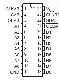 Specifications
Supply voltage range, VCC . . . . . . . . . . . . . . . . . . . . . . . . . . . . . . . . . . . . . . . . . . . . . 0.5 V to 4.6 V
Input voltage range, VI (see Note 1) . . . . . . . . . . . . . . . . . . . . . . . . . . . . . . . . . . . . . . 0.5 V to 7 V
Voltage range applied to any output in the high-impedance
or power-off state, VO (see Note 1). . . . . . . . . . . . . . . . . . . . . .. . . . . . . . . .. . . . . . . . 0.5 V to 7 V
Voltage range applied to any output in the high state, VO (see Note 1) . .. . . 0.5 V to VCC + 0.5 V
Current into any output in the low state, IO: SN54LVTH652 . . . . . . . . . . . . . . . . . . . . . . . . . . 96 mA
SN74LVTH652 . . . . . . . . . . . . . . . . . . . . . . . . . 128 mA
Current into any output in the high state, IO (see Note 2): SN54LVTH652 . . . . . . . . . . . . . . . . 48 mA
SN74LVTH652 . . . . . . . . . . . . . . . . 64 mA
Input clamp current, IIK (VI < 0) . . . . . . . . . . . . . . . . . . . . . . . . . . . . . . . . . . . . . . . . . . . . . . . 50 mA
Output clamp current, IOK (VO < 0) . . . . . . . . . . . . . . . . . . . . . . . . . . . . . . . . . . . . . . . . . . . . . 50 mA
Package thermal impedance, JA (see Note 3): DB package . . . . . . . . . . . . . . . . . . . . . . . . 104°C/W
DGV package . . . . . . . . . . . . . .. . . . . . . . . . 139°C/W
DW package . . . . . . . . . . . . . . . . . . . . . . . . . 81°C/W
PW package . . . . . . . . . . . . . . . . . . . . . . . . 120°C/W
Storage temperature range, Tstg . . . . . . . . . . . . . . . . . . . . . . .. .. . . . . .. . . . . . . . . . . 65°C to 150°
† Stresses beyond those listed under "absolute maximum ratings" may cause permanent damage to the device. These are stress ratings only, and functional operation of the device at these or any other conditions beyond those indicated under "recommended operating conditions" is not implied. Exposure to absolute-maximum-rated conditions for extended periods may affect device reliability NOTES: 1. The input and output negative-voltage ratings may be exceeded if the input and output clamp-current ratings are observed. 2. This current flows only when the utput is in the high state and VO > VCC. 3. The package thermal impedance is calculated in accordance with JESD 51
DescriptionThese bus transceivers and registers of LVTH652 are designed specifically for low-voltage (3.3-V) VCC operation, but with the capability to provide a TTL interface to a 5-V system environment.
The 'LVTH652 devices consist of bus-transceiver circuits, D-type flip-flops, and control circuitry arranged for multiplexed transmission of data directly from the data bus or from the internal storage registers.
Output-enable (OEAB and OEBA) inputs of LVTH652 are provided to control the transceiver functions. Select-control (SAB and SBA) inputs are provided to select whether real-time or stored data is transferred. The LVTH652 used for select control eliminates the typical decoding glitch that occurs in a multiplexer during the transition between real-time and stored data. A low input selects real-time data and a high input selects stored data. Figure 1 illustrates the four fundamental bus-management functions that can be performed with the 'LVTH652 devices.

 SN54LVTH652 Data Sheet


