Features: • State-of-the-Art Advanced BiCMOS Technology (ABT) Design for 3.3-V Operation and Low-Static Power Dissipation
• Supports Mixed-Mode Signal Operation (5-V Input and Output Voltages With 3.3-V VCC)
• Supports Unregulated Battery Operation Down to 2.7 V
• Typical VOLP (Output Ground Bounce) < 0.8 V at VCC = 3.3 V, TA = 25°C
• Latch-Up Performance Exceeds 500 mA Per JEDEC Standard JESD-17
• Bus-Hold Data Inputs Eliminate the Need for External Pullup Resistors
• Reduced Output Structure on A Port Minimizes VOHV
• Package Options Include Plastic Small-Outline (DW), Shrink Small-Outline (DB), and Thin Shrink Small-Outline (PW) Packages, Ceramic Chip Carriers (FK), and Ceramic DIPs (J)
Pinout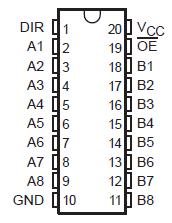 Specifications
Supply voltage range, VCC . . . . . . . . . . . . . . . . . . . . . . . . . . . . . . . . . . . . . . . . . . . . . . . .. . . 0.5 V to 4.6 V
Input voltage range, VI (see Note 1) . . . . . . . . . . . . . . . . . . . . . . . . . . . . . . . . . . . . . . . . . . . . 0.5 V to 7 V
Voltage range applied to any output in the high state or power-off state, VO (see Note 1) . . 0.5 V to 7 V
Current into any output in the low state, IO: SN54LVTR245 . . . . . . . . . . . . . . . . . . . . . . . . . . . . . . . . 96 mA
SN74LVTR245 . . . . . . . . . . . . . . . . . . . . . . . . . . . . . . . 128 mA
Current into any output in the high state, IO (see Note 2): SN54LVTR245 . . . . . . . . . . . . . . . . . . . .. 48 mA
SN74LVTR245 . . . . . . . . . . . . . . . . . . . . . 64 mA
Input clamp current, IIK (VI < 0) . . . . . . . . . . . . . . . . . . . . . . . . . . . . . . . . . . . . . . . . . . . . . . . . ... . . 50 mA
Output clamp current, IOK (VO < 0) . . . . . . . . . . . . . . . . . . . . . . . . . . . . . . . . . . . . . . . . . . . . .. . . . . 50 mA
Maximum power dissipation at TA = 55°C (in still air): DB package . . . . . . . . . . . . . . . . . . . . . . . . . . 0.65 W
DW package . . . . . . . . . . . . . . . . . . . . . . . . .. 0.85 W
PW package . . . . . . . . . . . . . . . . . . . . . . . . . . 0.6 W
Storage temperature range . . . . . . . . . . . . . . . . . . . . . . . . . . . . . . . . . . . . . . . . . . . . . . . . 65°C to 150°C
‡ Stresses beyond those listed under "absolute maximum ratings" may cause permanent damage to the device. These are stress ratings only, and functional operation of the device at these or any other conditions beyond those indicated under "recommended operating conditions" is not implied. Exposure to absolute-maximum-rated conditions for extended periods may affect device reliability.
NOTES: 1. The input and output negative-voltage ratings may be exceeded if the input and output clamp-current ratings are observed.
2. This current will only flow when the output is in the high state and VO > VCC.
DescriptionThese octal bus transceivers SN54LVTR245 are designed specifically for low-voltage (3.3-V) VCC operation, but with the capability to provide a TTL interface to a 5-V system environment.
The 4LVTR245 is designed for asynchronous communication between data buses. The SN54LVTR245 transmits data from the A bus to the B bus or from the B bus to the A bus depending upon the logic level at the direction-control (DIR) input. The output-enable (OE) input can be used to disable the SN54LVTR245 so the buses are effectively isolated. Active bus-hold circuitry is provided to hold unused or floating data inputs at a valid logic level. The A port is designed to minimize the undershoot exhibited on high to low transition during simultaneous switching conditions.
The SN74LVTR245 is available in TI's shrink small-outline package (DB), which provides the same I/O pin count and functionality of standard small-outline packages in less than half the printed-circuit-board area.
The SN54LVTR245 is characterized for operation over the full military temperature range of 55°C to 125°C. The SN74LVTR245 is characterized for operation from 40°C to 85°C.

 SN54LVTR245 Data Sheet


