Features: ·Single 5-V Supply
·3-State Driver Output Circuitry
·TTL-Compatible Driver Inputs
·TTL-Compatible Receiver Output
· Differential Line Operation
· Receiver Output Strobe (SN55116,
SN75116, SN75117) or Enable (SN75118,
SN75119)
· Designed for Party-Line (Data-Bus) Applications
· Choice of Ceramic or Plastic Packages
· Independent Driver and Receiver
· Choice of Open-Collector or Totem-Pole Outputs on Both Driver and Receiver
· Dual Data Inputs on Driver
· Optional Line-Termination Resistor in Receiver
· ±15-V Receiver Common-Mode Capability
· Receiver Frequency-Response Control
· Driver Output Internally Connected to Receiver InputPinout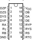 SpecificationsSupply voltage, VCC (see Notes 1 and 2) . . . . . . . . . . . . . . . . . . . . . . . . . . . . . . . . . . . . . . . . . . . . .. . 7 V
Input voltage, VI: DA, DB, DE, DI, RE, and RS . . . . . . . . . . . . . . . . . . . . . . . . . . . . . . . . . . . . . . . . . . 5.5 V
RA, RB, RT for '116, SN75118 only . . . . . . . . . . . . . . . . . . . . . . . . . . . . . . . . . . ±25 V
A and B for SN75117, SN75119 only . . . . . . . . . . . . . . . . . . . . . . . . . . . . . . . . 0 to 6 V
Off-state voltage applied to open-collector outputs: '116, SN75118 only . . . . . . . . . . . . . . . . .. . . . 12 V
Continuous total power dissipation (see Note 2) . . . . . . . . . . . . . . . . . . . . . See Dissipation Rating Table
Storage temperature range, Tstg . . . . . . . . . . . . . . . . . . . . . . . . . . . . . . . . . . . . . . . . . 65°C to 150°C
Case temperature for 60 seconds, TC: FK package . . . . . . . . . . . . . . . . . . . . . . . . . . . . . . . . . .. . . 260°C
Lead temperature 1,6 mm (1/16 inch) from case for 60 seconds: J package . . . . . . . . . . . . . . . . . 300°C
Lead temperature 1,6 mm (1/16 inch) from case for 10 seconds: D, N, or P package . . . . . . . . . . . 260°C
‡ Stresses beyond those listed under "absolute maximum ratings" may cause permanent damage to the device. These are stress ratings only, and functional operation of the device at these or any other conditions beyond those indicated under "recommended operating conditions" is not implied. Exposure to absolute-maximum-rated conditions for extended periods may affect device reliability.
NOTES: 1. All voltage values are with respect to the network ground terminal.
2. In the FK and J packages, the SN55116 chip is alloy mounted. The SN75116, SN75117, SN75118,
and SN75119 chips are glass mounted.DescriptionThese integrated circuits are designed for use in interfacing between TTL-type digital systems and differential data-transmission lines. SN55116, SN75116, and SN75118 are especially useful for party-line (data-bus) applications. Each of SN55116, SN75116, and SN75118 combine in one package a 3-state differential line driver and a differential-input line receiver, both of which operate from a single 5-V power supply. The driver inputs and the receiver outputs are TTL compatible. The driver employed is similar to the SN55113 and SN75113 3-state line drivers, and the receiver is similar to the SN55115 and SN75115 line receivers.
The SN55116, SN75116, and SN75118 offer all the features of the SN55113 and SN75113 drivers and the SN55115 and SN75115 receivers combined. The driver performs the dual input AND and NAND functions when enabled or presents a high impedance to the load when in the disabled state. The driver output stages are similar to TTL totem-pole outputs, but have the current-sinking portion separated from the current-sourcing portion and both are brought out to adjacent package terminals. SN55116, SN75116, and SN75118 feature allows the user the option of using the driver in the open-collector output configuration, or, by connecting the adjacent source and sink terminals together, of using the driver in the normal totem-pole output configuration.
The receiver portion of the SN55116, SN75116, and SN75118 features a differential-input circuit having a common-mode voltage range of ±15 V. An internal 130- equivalent resistor also is provided, which optionally can be used to terminate the transmission line. A frequency-response control terminal allows the user to reduce the speed of the receiver or to improve differential noise immunity. The receivers of the SN55116 and SN75116 have an output strobe and a split totem-pole output. The receiver of the SN75118 has an output-enable for the 3-state split totem-pole output. The receiver section of either circuit is independent of the driver section except for the VCC and ground terminals.
The SN75117 and SN75119 provide the basic driver and receiver functions of the SN55116, SN75116, and SN75118, but use a package that is only half as large. The SN75117 and SN75119 are intended primarily for party-line or bus-organized systems because the driver outputs are internally connected to the receiver inputs. The driver has a single data input and a single enable input. The SN75117 receiver has an output strobe, while the SN75119 receiver has a 3-state output enable. However, SN55116, SN75116, and SN75118 do not provide output connection options, line-termination resistors, or receiver frequency-response controls.

 SN55116 Data Sheet