SN65CML100

Features: · Provides Level Translation From LVDS or LVPECL to CML, Repeating From CML to CML· Signaling Rates1 up to 1.5 Gbps· CML Compatible Output Directly Drives Devices With 3.3-V, 2.5-V, or 1.8-V Supplies· Total Jitter < 70 ps· Low 100 ps (Max) Part-To-Part Skew· Wide Common-Mode Receiver ...

product image

SN65CML100 Picture
SeekIC No. : 004497357 Detail

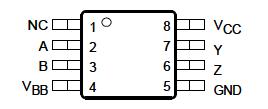
SN65CML100: Features: · Provides Level Translation From LVDS or LVPECL to CML, Repeating From CML to CML· Signaling Rates1 up to 1.5 Gbps· CML Compatible Output Directly Drives Devices With 3.3-V, 2.5-V, or 1.8...

floor Price/Ceiling Price

Part Number:
SN65CML100
Supply Ability:
5000

Price Break

  • Qty
  • 1~5000
  • Unit Price
  • Negotiable
  • Processing time
  • 15 Days
Total Cost: $ 0.00

SeekIC Buyer Protection PLUS - newly updated for 2013!

  • Escrow Protection.
  • Guaranteed refunds.
  • Secure payments.
  • Learn more >>

Month Sales

268 Transactions

Rating

evaluate  (4.8 stars)

Upload time: 2025/12/24

Payment Methods

All payment methods are secure and covered by SeekIC Buyer Protection PLUS.

Notice: When you place an order, your payment is made to SeekIC and not to your seller. SeekIC only pays the seller after confirming you have received your order. We will also never share your payment details with your seller.
Product Details

Description


Features:

· Provides Level Translation From LVDS or LVPECL to CML, Repeating From CML to CML
· Signaling Rates1 up to 1.5 Gbps
· CML Compatible Output Directly Drives Devices With 3.3-V, 2.5-V, or 1.8-V Supplies
· Total Jitter < 70 ps
· Low 100 ps (Max) Part-To-Part Skew
· Wide Common-Mode Receiver Capability Allows Direct Coupling of Input Signals
· 25 mV of Receiver Input Threshold Hysteresis Over 0-V to 4-V Common-Mode Range
· Propagation Delay Times, 800 ps Maximum
· 3.3-V Supply Operation
· Available in SOIC and MSOP Packages


Application

· Level Translation
· 622-MHz Central Office Clock Distribution
· High-Speed Network Routing
· Wireless Basestations
· Low Jitter Clock Repeater


Pinout

  Connection Diagram


Specifications

over operating free-air temperature range unless otherwise noted(1)

  UNIT
Supply voltage range,(2) VCC 0.5 V to 4 V
Sink/source, IBB ±0.5 mA
Voltage range, (A, B, Y, Z) 0 V to 4.3 V
Electrostatic discharge
Electrostaticdischarge
Human Body Model(3) A, B, Y, Z, and GND ±5 kV
All pins ±2 kV
Charged-Device Model(4) All pins ±1500 V
Continuous power dissipation See Dissipation Rating Table
Storage temperature range, Tstg 65°C to 150°C
Lead temperature 1,6 mm (1/16 inch) from case for 10 seconds 260°C

(1) Stresses beyond those listed under "absolute maximum ratings" may cause permanent damage to the device. These are stress ratings only, and functional operation of the device at these or any other conditions beyond those indicated under "recommended operating conditions" is not implied. Exposure to absolute-maximum-rated conditions for extended periods may affect device reliability.
(2) All voltage values, except differential I/O bus voltages, are with respect to network ground terminal.
(3) Tested in accordance with JEDEC Standard 22, Test Method A114-A.7.
(4) Tested in accordance with JEDEC Standard 22, Test Method C101.


Description

This high-speed translator/repeater SN65CML100 is designed for signaling rates up to 1.5 Gbps to support various high-speed network routing applications. The driver output is compatible with current-mode logic (CML) levels, and directly drives 50- or 25- loads connected to 1.8-V, 2.5-V, or 3.3-V nominal supplies. The capability for direct connection to the loads may eliminate the need for coupling capacitors. The receiver SN65CML100 input is compatible with LVDS (TIA/EIA644), LVPECL, and CML signaling levels. The receiver tolerates a wide common-mode voltage range, and SN65CML100 may also be directly coupled to the signal source. The internal data path from input to output is fully differential for low noise generation and low pulse-width distortion.

The VBB pin of SN65CML100 is an internally generated voltage supply to allow operation with a single-ended LVPECL input. For single-ended LVPECL input operation, the unused differential input is connected to VBB as a switching reference voltage. When used, decouple VBB with a 0.01-F capacitor and limit the current sourcing or sinking to 400 A. When not used, VBB should be left open.

SN65CML100 is characterized for operation from 40°C to 85°C.


Customers Who Bought This Item Also Bought

Margin,quality,low-cost products with low minimum orders. Secure your online payments with SeekIC Buyer Protection.
View more