Features: ` Operates With a 3.3-V Supply
` Bus-Pin ESD Protection Exceeds 16 kV HBM
` 1/8 Unit-Load Option Available (Up to 256 Nodes on the Bus)
` Optional Driver Output Transition Times for Signaling Rates† of 1 Mbps, 10 Mbps and 25 Mbps
` Meets or Exceeds the Requirements of ANSI TIA/EIA-485-A
` Bus-Pin Short Circuit Protection From 7 V to 12 V
` Low-Current Standby Mode . . . 1 µA Typical
` Open-Circuit, Idle-Bus, and Shorted-Bus Failsafe Receiver
` Thermal Shutdown Protection
` Glitch-Free Power-Up and Power-Down Protection for Hot-Plugging Applications
` SN75176 Footprint APPLICATIONS
` Digital Motor Control
` Utility Meters
` Chassis-to-Chassis Interconnects
` Electronic Security Stations
` Industrial Process Control
` Building Automation
` Point-of-Sale (POS) Terminals and NetworksApplication· Digital Motor Control
· Utility Meters
· Chassis-to-Chassis Interconnects
· Electronic Security Stations
· Industrial Process Control
· Building Automation
· Point-of-Sale (POS) Terminals and NetworksPinout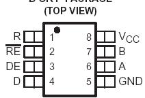 Specifications
|
|
SN65HVD10, SN75HVD10
SN65HVD11, SN75HVD11
SN65HVD12, SN75HVD12 |
|
Supply voltage range, VCC |
-0.3 V to 6V |
|
Voltage range at A or B |
-9 V to 14 V |
|
Input voltage range at D, DE, R or RE |
−0.5 V to VCC + 0.5 V |
|
Voltage input range, transient pulse, A and B, through 100 Ω (see Figure 11) |
−50 V to 50 V |
|
Electrostatic discharge |
Human Body Model (3) |
A, B and GND |
14 kV |
| All pins |
6 kV |
| Charged-Device Model (4) |
All pins |
1 kV |
|
Continuous total power dissipation |
(see Dissipation Rating
Table) |
|
Junction temperature, TJ |
170°C |
|
Storage temperature range, Tstg |
-65C to 150°C |
|
Lead temperature 1,6 mm (1/16 inch) from case for 10 seconds |
260°C |
(1) Stresses beyond those listed under "absolute maximum ratings" may cause permanent damage to the device. These are stress ratings
only and functional operation of the device at these or any other conditions beyond those indicated under "recommended operating
conditions" is not implied. Exposure to absolute-maximum-rated conditions for extended periods may affect device reliability.
(2) All voltage values, except differential I/O bus voltages, are with respect to network ground terminal.
(3) Tested in accordance with JEDEC Standard 22, Test Method A114-A.
(4) Tested in accordance with JEDEC Standard 22, Test Method C101.
DescriptionThe SN65HVD10, SN75HVD10, SN65HVD11, SN75HVD11, SN65HVD12, and SN75HVD12 combine a 3-state differential line driver and differential input line receiver that operate with a single 3.3-V power supply. SN65HVD10, SN75HVD10, SN65HVD11, SN75HVD11, SN65HVD12, and SN75HVD12 are designed for balanced transmission lines and meet or exceed ANSI standard TIA/EIA-485-A and ISO 8482:1993. These differential bus transceivers are monolithic integrated circuits designed for bidirectional data communication on multipoint bus-transmission lines. The drivers and receivers have active-high and active-low enables respectively, that can be externally connected together to function as direction control. Very low device standby supply current can be achieved by disabling the driver and the receiver.
The driver differential outputs and receiver differential inputs of SN65HVD10, SN75HVD10, SN65HVD11, SN75HVD11, SN65HVD12, and SN75HVD12 connect internally to form a differential input/ output (I/O) bus port that is designed to offer minimum loading to the bus whenever the driver is disabled or VCC = 0. SN65HVD10, SN75HVD10, SN65HVD11, SN75HVD11, SN65HVD12, and SN75HVD12 feature wide positive and negative common-mode voltage ranges, making them suitable for party-line applications.

 SN65HVD11 Data Sheet


