Features: · 1/8 Unit-Load Option Available (Up to 256 Nodes on the Bus)
· Bus-Pin ESD Protection Exceeds 15 kV HBM
· Optional Driver Output Transition Times for Signaling Rates (1) of 1 Mbps, 5 Mbps and 25 Mbps
· Low-Current Standby Mode: < 1 mA
· Glitch-Free Power-Up and Power-Down Protection for Hot-Plugging Applications
· 5V Tolerant Inputs
· Bus Idle, Open, and Short Circuit Failsafe
· Meets or exceeds the requirements of ANSI TIA/EIA-485-A and RS-422 Compatible
· 5-V Devices available, SN65HVD50-59Application· Utility Meters
· DTE/DCE Interfaces
· Industrial, Process, and Building Automation
· Point-of-Sale (POS) Terminals and NetworksPinout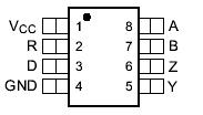 Specifications
|
|
|
UNIT |
|
VCC |
Supply voltage range, VCC |
0.3 V to 6 V |
|
|
Voltage range at any bus terminal (A, B, Y, Z) |
9 V to 14 V |
|
|
Voltage input, transient pulse through 100 W. See Figure 12 (A, B, Y, Z)(3) |
50 to 50 V |
|
VI |
Input voltage range (D, DE, RE) |
-0.5 V to 7 V |
|
|
Continuous total power dissipation |
Internally limited |
|
IO |
Output current (receiver output only, R) |
11 mA |
(1) Stresses beyond those listed under absolute maximum ratings may cause permanent damage to the device. These are stress ratings
only, and functional operation of the device at these or any other conditions beyond those indicated under recommended operating
conditions is not implied. Exposure to absolute-maximum-rated conditions for extended periods may affect device reliability.
(2) All voltage values, except differential I/O bus voltages, are with respect to network ground terminal.
(3) This tests survivability only and the output state of the receiver is not specified.
DescriptionThe SN65HVD3X devices are 3-state differential line drivers and differential-input line receivers that operate with 3.3-V power supply.Each driver and receiver has separate input and output pins for full-duplex bus communication designs. SN65HVD3X is designed for balanced transmission lines and interoperation with ANSI TIA/EIA-485A, TIA/EIA-422-B, ITU-T v.11 and ISO 8482:1993 standard-compliant devices.
The SN65HVD30, SN65HVD31, SN65HVD32, SN65HVD36 and SN65HVD37 are fully enabled with no external enabling pins. The SN65HVD36 and SN65HVD37 implement receiver equalization technology for improved performance in long distance applications.
The SN65HVD33, SN65HVD34, SN65HVD35, SN65HVD38, and SN65HVD39 have active-high driver enables and active-low receiver enables. A very low, less than 1 mA, standby current can be achieved by disabling both the driver and receiver.
The SN65HVD38 and SN65HVD39 implement receiver equalization technology for improved performance in long distance applications.
SN65HVD30, SN65HVD31, SN65HVD32, SN65HVD36 and SN65HVD37 are characterized for operation from -40°C to +85°C.
The SN65HVD36 and SN65HVD38 implement receiver equalization technology for improved jitter performance on differential bus applications with data rates up to 20 Mbps at cable lengths up to 160 meters.The SN65HVD37 and SN65HVD39 implement receiver equalization technology for improved jitter performance on differential bus applications with data rates in the range of 1 to 5 Mbps at cable lengths up to 1000 meters.This integrated circuit can be damaged by ESD. Texas Instruments recommends that SN65HVD30, SN65HVD31, SN65HVD32, SN65HVD36 and SN65HVD37 are handled with appropriate precautions. Failure to observe proper handling and installation procedures can cause damage.
ESD damage can range from subtle performance degradation to complete device failure. Precision integrated circuits of SN65HVD30, SN65HVD31, SN65HVD32, SN65HVD36 and SN65HVD37 may be more susceptible to damage because very small parametric changes could cause the device not to meet its published specifications.

 SN65HVD30-SN65HVD35 Data Sheet


