Features: ` Three Differential Transceivers in One Package
` Signaling Rates1 Up to 30 Mbps
` Low Power and High Speed
` Designed for TIA/EIA-485, TIA/EIA-422, ISO 8482, and ANSI X3.277 (HVD SCSI Fast20) Applications
` Common-Mode Bus Voltage Range 7 V to 12 V
` ESD Protection on Bus Terminals Exceeds 12 kV
` Driver Output Current up to ±60 mA
` Thermal Shutdown Protection
` Driver Positive and Negative Current Limiting
` Power-Up, Power-Down Glitch-Free Operation
` Pin-Compatible With the SN75ALS171
` Available in Shrink Small-Outline PackagePinout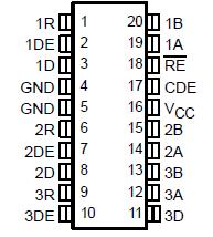 Specifications
Supply voltage, VCC (see Note 1) . . . . . . . . . . . . . . . . . . . . . . . . . . . . . . . . . . . . . . . . . . 0.3 V to 6 V
Voltage range at any bus I/O terminal (steady state) . . . . . . . . . . . . . . . . . . . . . . . . . . 10 V to 15 V
Voltage input range, A and B, (transient pulse through 100 , see Figure 12) . . . . . .. 30 V to 30 V
Voltage range at any DE, RE, or CDE terminal . . . . . . . . . . . . . . . . . . . . . . . . . 0.5 V to VCC + 0.5 V
Electrostatic discharge: Human body model (A, B, GND) (see Note 2) . . . . . . . . . . . . . . . . . . . . . 12 kV
All pins . . . . . . . . . . . . . . . . . . . . . . . . . . . . . . . . . . . . . . . . . . . . . . . . . . . 5 kV
Charged-device model (all pins) (see Note 3) . . . . . . . . . . . . . . . . .. . . . . 1 kV
Continuous total power dissipation . . . . . . . . . . . . . . . . . . . . . .. . See Power Dissipation Rating Table
Storage temperature range, Tstg . . . . . . . . . . . . . . . . . . . . . . . . . . . . . . . . . . . . . . . 65°C to 150°C
Lead temperature 1,6 mm (1/16 inch) from case for 10 seconds . . . . . . . . . . . . . . . . . . . . . . . . 260°C
† Stresses beyond those listed under "absolute maximum ratings" may cause permanent damage to the device. These are stress ratings only, and functional operation of the device at these or any other conditions beyond those indicated under "recommended operating conditions" is not implied. Exposure to absolute-maximum-rated conditions for extended periods may affect device reliability.
NOTES: 1. All voltage values, except differential I/O bus voltages, are with respect to network ground terminal.
2. Tested in accordance with JEDEC Standard 22, Test Method A114A.
3. Tested in accordance with JEDEC Standard 22, Test Method C101.
DescriptionThe SN65LBC171 and SN75LBC171 are monolithic integrated circuits designed for bidirectional data communication on multipoint bus-transmission lines. Potential applications include serial or parallel data transmission, cabled peripheral buses with twin axial, ribbon, or twisted-pair cabling. SN65LBC171 and SN75LBC171 are suitable for FAST20 SCSI and can transmit or receive data pulses as short as 25 ns, with skew less than 3 ns.
SN65LBC171 and SN75LBC171 combine three 3-state differential line drivers and three differential input line receivers, all of which operate from a single 5-V power supply.
The driver differential outputs and the receiver differential inputs of SN65LBC171 and SN75LBC171 are connected internally to form three differential input/output (I/O) bus ports that are designed to offer minimum loading to the bus whenever the driver is disabled or VCC = 0. SN65LBC171 and SN75LBC171 feature a wide common-mode voltage range making the device suitable for party-line applications over long cable runs.
The SN75LBC171 is characterized for operation over the temperature range of 0°C to 70°C. The SN65LBC171 is characterized for operation over the temperature range of 40°C to 85°C.

 SN65LBC171 Data Sheet


