SN65LV1021

Features: ` 100-Mbps to 400-Mbps Serial LVDS Data Payload Bandwidth at 10-MHz to 40-MHz System Clock` Pin-Compatible Superset of NSM DS92LV1021/DS92LV1212` Chipset (Serializer/Deserializer) Power Consumption <350 mW (Typ) at 40 MHz` Synchronization Mode for Faster Lock` Lock Indicator` No Exter...

product image

SN65LV1021 Picture
SeekIC No. : 004497426 Detail

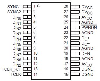
SN65LV1021: Features: ` 100-Mbps to 400-Mbps Serial LVDS Data Payload Bandwidth at 10-MHz to 40-MHz System Clock` Pin-Compatible Superset of NSM DS92LV1021/DS92LV1212` Chipset (Serializer/Deserializer) Power Co...

floor Price/Ceiling Price

Part Number:
SN65LV1021
Supply Ability:
5000

Price Break

  • Qty
  • 1~5000
  • Unit Price
  • Negotiable
  • Processing time
  • 15 Days
Total Cost: $ 0.00

SeekIC Buyer Protection PLUS - newly updated for 2013!

  • Escrow Protection.
  • Guaranteed refunds.
  • Secure payments.
  • Learn more >>

Month Sales

268 Transactions

Rating

evaluate  (4.8 stars)

Upload time: 2025/12/24

Payment Methods

All payment methods are secure and covered by SeekIC Buyer Protection PLUS.

Notice: When you place an order, your payment is made to SeekIC and not to your seller. SeekIC only pays the seller after confirming you have received your order. We will also never share your payment details with your seller.
Product Details

Description


Features:

` 100-Mbps to 400-Mbps Serial LVDS Data Payload Bandwidth at 10-MHz to 40-MHz System Clock
` Pin-Compatible Superset of NSM DS92LV1021/DS92LV1212
` Chipset (Serializer/Deserializer) Power Consumption <350 mW (Typ) at 40 MHz
` Synchronization Mode for Faster Lock
` Lock Indicator
` No External Components Required for PLL
` Low-Cost 28-Pin SSOP Package
` Industrial Temperature Qualified, TA = 40°C to 85°C
` Programmable Edge Trigger on Clock (Rising or Falling Edge)
` Flow-Through Pinout for Easy PCB Layout


Pinout

  Connection Diagram


Specifications

VCC to GND . . . . . . . . . . . . . . . . . . . . . . . . . . . . . . . . . . . . . . . . . . . . . . . . . . . . . .  . . . . . . . . . 0.3 V to 4 V
LVTTL input voltage . . . . . . . . . . . . . . . . . . . . . . . . . . . . . . . . . . . . . . . . . . . . . .  . . . 0.3 V to (VCC + 0.3 V)
LVTTL output voltage . . . . . . . . . . . . . . . . . . . . . . . . . . . . . . . . . . . . . . . . . . . . . . . . 0.3 V to (VCC + 0.3 V)
LVDS receiver input voltage . . . . . . . . . . . . . . . . . . . . . . . . . . . . . . . . . . . . . . . . . . . . .. . . . . 0.3 V to 3.9 V
LVDS driver output voltage . . . . . . . . . . . . . . . . . . . . . . . . . . . . . . . . . . . . . . . . . . . . . . . . . . 0.3 V to 3.9 V
LVDS output short circuit duration . . . . . . . . . . . . . . . . . . . . . . . . . . . . . . . . . . . . . . . . . . . . . . . . Continuous
Electrostatic discharge: HBM . . . . . . . . . . . . . . . . . . . . . . . . . . . . . . . . . . . . . . . . . . . . . . . . . . . . . up to 6 kV
                                      MM . . . . . . . . . . . . . . . . . . . . . . . . . . . . . . . . . . . . . . . . . . . . . . . . .  . . . up to 200 V
Junction temperature . . . . . . . . . . . . . . . . . . . . . . . . . . . . . . . . . . . . . . . . . . . . . . . . . . . . . . . . . . . . . 150°C
Storage temperature . . . . . . . . . . . . . . . . . . . . . . . . . . . . . . . . . . . . . . . . . . . . . . . . . . . . 65°C to 150°C
Lead temperature (soldering, 4 seconds) . . . . . . . . . . . . . . . . . . . . . . . . . . . . . . . . . . . . . .. . . . . . . . 260°C
Maximum package power dissipation, TA = 25°C . . . . . . . . . . . . . . . . . . . . . . . . . . . . .. . . . . . . . . . . 1.27 W
Package derating . . . . . . . . . . . . . . . . . . . . . . . . . . . . . . . . . . . . . . . . . . . . .. . . .  10.3 mW/°C above 25°C

† Stresses beyond those listed under "absolute maximum ratings" may cause permanent damage to the device. These are stress ratings only, and functional operation of the device at these or any other conditions beyond those indicated under "recommended operating conditions" is not implied. Exposure to absolute-maximum-rated conditions for extended periods may affect device reliability.


Description

The SN65LV1021 serializer and SN65LV1212 deserializer comprise a 10-bit serdes chipset designed to transmit and receive serial data over LVDS differential backplanes at equivalent parallel word rates from 10 MHz to 40 MHz. Including overhead,SN65LV1021 translates into a serial data rate between 120-Mbps and 480-Mbps payload-encoded throughput.

Upon power up, the chipset link can be initialized via a synchronization mode with internally generated SYNC patterns, or the deserializer SN65LV1021 can be allowed to synchronize to random data. By using the synchronization mode, the deserializer SN65LV1021 establishes lock within specified, shorter time parameters.

The SN65LV1021 can be entered into a power-down state when no data transfer is required. Alternatively, a mode is available to place the output pins in the high-impedance state without losing PLL lock.

The SN65LV1021 and SN65LV1212 are characterized for operation over ambient air temperature of 40°C to 85°C.


Customers Who Bought This Item Also Bought

Margin,quality,low-cost products with low minimum orders. Secure your online payments with SeekIC Buyer Protection.
Undefined Category
Power Supplies - External/Internal (Off-Board)
Connectors, Interconnects
Semiconductor Modules
View more