Features: · Receiver Equalization and Selectable Driver Preemphasis to Counteract High-Frequency Transmission Line Losses
· Integration of Two-Serial Port
· Selectable Loopback
· Typical Power Consumption 650 mW
· 30-ps Deterministic Jitter
· On-Chip 100-W Receiver and Driver Differential Termination Resistors Eliminate External Components and Reflection from Stubs
· 3.3-V Nominal Power Supply
· 48-Terminal QFN (Quad Flatpack No-lead) 7 mm × 7 mm × 1 mm, 0.5-mm Terminal PitchApplication· Bidirectional Link Replicator
· Signal Conditioner
· XAUI 802.3ae Protocol Backplane Redundancy
· Host Adapter (Applications With Internal and External Connection to SERDES)
· Signaling Rates DC to 4 Gbps Including XAUI, GbE, FC, HDTVPinout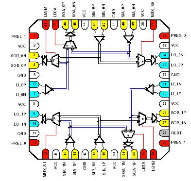 Specifications
|
|
UNIT |
|
VCC Supply voltage range(2) |
−0.5 V to 6V |
|
Voltage range |
Control inputs, all outputs |
0.5 V to (VCC + 0.5 V) |
|
Receiver inputs |
−0.5 V to 4 V |
|
ESD |
Human Body Model(3) |
All pins |
4 kV |
|
Charged-Device Model(4) |
All pins |
500V |
|
Continuous power dissipation |
See Dissipation Rating Table |
|
Moisture sensitivity level |
2 |
|
Reflow temperature package soldering, 4 seconds |
260°C |
(1) Stresses beyond those listed under absolute maximum ratings may cause permanent damage to the device. These are stress ratings
only and functional operation of the device at these or any other conditions beyond those indicated under recommended operating
conditions is not implied. Exposure to absolute-maximum-rated conditions for extended periods may affect device reliability.
(2) All voltage values, except differential I/O bus voltages, are with respect to network ground terminal.
(3) Tested in accordance with JEDEC Standard 22, Test Method A114-A.
(4) Tested in accordance with JEDEC Standard 22, Test Method C101.
DescriptionThe SN65LVCP40 is a signal conditioner and data multiplexer optimized for backplanes. Input equalization and programmable output preemphasis support data rates up to 4 Gbps. Common applications are redundancy switching, signal buffering, or performance improvements on legacy backplane hardware.
The SN65LVCP40 combines a pair of 1:2 buffers with a pair of 2:1 multiplexers (mux). Selectable switch-side loopback supports system testing. System interconnects and serial backplane applications of up to 4 Gbps are supported. Each of the two independent channels consists of a transmitter SN65LVCP40 with a fan-out of two, and a receiver with a 2:1 input multiplexer.
The drivers provide four selectable levels of preemphasis to compensate for transmission line losses. The receivers incorporates receive equalization and compensates for input transmission line loss. SN65LVCP40 minimizes deterministic jitter in the link. The equalization is optimized to compensate for a FR-4 backplane trace with 5-dB, high-frequency loss between 375 MHz and 1.875 MHz. SN65LVCP40 corresponds to a 24-inch long FR-4 trace with 6-mil trace width.
SN65LVCP40 operates from a single 3.3-V supply. The device has integrated 100-W line termination and provides self-biasing. The input tolerates most differential signaling levels such as LVDS, LVPECL or CML. The output impedance matches 100-W line impedance. The inputs and outputs of SN65LVCP40 may be ac coupled for best interconnectivity with other devices such as SERDES I/O or additional XAUI multiplexer buffer. With ac coupling, jitter is the lowest.

 SN65LVCP40 Data Sheet


