SN65LVDS049

Features: · DS90LV049 Compatible· Up to 400 Mbps Signaling Rates· Flow-Through Pin-out· 50 ps Driver Channel-to-Channel Skew (Typ)· 50 ps Receiver Channel-to-Channel Skew(Typ)· 3.3-V Power Supply· High-Impedance Disable for all Outputs· Internal Failsafe Biasing of Receiver Inputs· 1.4 ns Driver P...

product image

SN65LVDS049 Picture
SeekIC No. : 004497450 Detail

SN65LVDS049: Features: · DS90LV049 Compatible· Up to 400 Mbps Signaling Rates· Flow-Through Pin-out· 50 ps Driver Channel-to-Channel Skew (Typ)· 50 ps Receiver Channel-to-Channel Skew(Typ)· 3.3-V Power Supply· H...

floor Price/Ceiling Price

Part Number:
SN65LVDS049
Supply Ability:
5000

Price Break

  • Qty
  • 1~5000
  • Unit Price
  • Negotiable
  • Processing time
  • 15 Days
Total Cost: $ 0.00

SeekIC Buyer Protection PLUS - newly updated for 2013!

  • Escrow Protection.
  • Guaranteed refunds.
  • Secure payments.
  • Learn more >>

Month Sales

268 Transactions

Rating

evaluate  (4.8 stars)

Upload time: 2025/12/24

Payment Methods

All payment methods are secure and covered by SeekIC Buyer Protection PLUS.

Notice: When you place an order, your payment is made to SeekIC and not to your seller. SeekIC only pays the seller after confirming you have received your order. We will also never share your payment details with your seller.
Product Details

Description


Features:

· DS90LV049 Compatible
· Up to 400 Mbps Signaling Rates
· Flow-Through Pin-out
· 50 ps Driver Channel-to-Channel Skew (Typ)
· 50 ps Receiver Channel-to-Channel Skew(Typ)
· 3.3-V Power Supply
· High-Impedance Disable for all Outputs
· Internal Failsafe Biasing of Receiver Inputs
· 1.4 ns Driver Propagation Delay (Typ)
· 1.9 ns Receiver Propagation Delay (Typ)
· High Impedance Bus Pins on Power Down
· ANSI TIA/EIA-644-A Compliant
· Receiver Input and Driver Output ESD Exceeds 10 kV
· 16-pin TSSOP Package


Application

· Full-duplex LVDS Communications of Clock and Data
· Printers


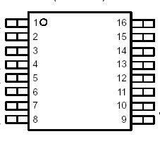
Pinout

  Connection Diagram


Specifications

UNIT

Supply voltage(2), VCC

0.3 V to 4 V

Voltage range  DIN, ROUT, EN, or EN

-0.3 V to (VCC + 0.3 V)

RIN+ or RIN-

-0.3 V to 4 V

 DOUT+ or DOUT-

 -0.3 V to 3.9 V

ESD

Human Body Model(3) RIN+, RIN-, DOUT+, and DOUT-

±10 kV

All pins ±2 kV
Charged-Device Model(4) All pins ±500 V

LVDS output short circuit duration (DOUT+, DOUT-)

Continuous

Continuous power dissipation

 See Dissipation Rating Table

Storage temperature range

 -65°C to 150°C

Lead temperature 1,6 mm (1/16 inch) from case for 10 seconds

 260

(1) Stresses beyond those listed under absolute maximum ratings may cause permanent damage to the device. These are stress ratings only, and functional operation of the device at these or any other conditions beyond those indicated under recommended operating conditions is not implied. Exposure to absolute-maximum-rated conditions for extended periods may affect device reliability.

(2) All voltage values, except differential I/O bus voltages, are with respect to network ground terminal.

(3) Tested in accordance with JEDEC Standard 22, Test Method A114-A.

(4) Tested in accordance with JEDEC Standard 22, Test Method C101.


Description

The SN65LVDS049 is a dual flow-through differential line driver-receiver pair that uses low-voltage differential signaling (LVDS) to achieve signaling rates as high as 400 Mbps. The TIA/EIA-644-A standard compliant electrical interface SN65LVDS049 provides a minimum differential out-put voltage magnitude of 250 mV into a 100- load and receipt of signals with up to 1 V of ground potential difference between a transmitter and receiver. The LVDS receivers have internal failsafe biasing that places the outputs into a known high state for unconnected differential inputs.


Customers Who Bought This Item Also Bought

Margin,quality,low-cost products with low minimum orders. Secure your online payments with SeekIC Buyer Protection.
Soldering, Desoldering, Rework Products
Transformers
Cables, Wires
Inductors, Coils, Chokes
Optical Inspection Equipment
Memory Cards, Modules
View more