SN65LVDS117

ApplicationThe SN65LVDS109 and SN65LVDS117 devices solve several problems common to the distribution of timing critical clock and data signals. These problems include:`Excessive skew between the signals`Noise pickup over long signaling paths`High power consumption`Control of which signal paths are...

product image

SN65LVDS117 Picture
SeekIC No. : 004497464 Detail

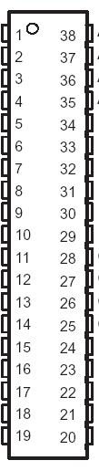
SN65LVDS117: ApplicationThe SN65LVDS109 and SN65LVDS117 devices solve several problems common to the distribution of timing critical clock and data signals. These problems include:`Excessive skew between the sig...

floor Price/Ceiling Price

Part Number:
SN65LVDS117
Supply Ability:
5000

Price Break

  • Qty
  • 1~5000
  • Unit Price
  • Negotiable
  • Processing time
  • 15 Days
Total Cost: $ 0.00

SeekIC Buyer Protection PLUS - newly updated for 2013!

  • Escrow Protection.
  • Guaranteed refunds.
  • Secure payments.
  • Learn more >>

Month Sales

268 Transactions

Rating

evaluate  (4.8 stars)

Upload time: 2025/12/24

Payment Methods

All payment methods are secure and covered by SeekIC Buyer Protection PLUS.

Notice: When you place an order, your payment is made to SeekIC and not to your seller. SeekIC only pays the seller after confirming you have received your order. We will also never share your payment details with your seller.
Product Details

Description


Application

The SN65LVDS109 and SN65LVDS117 devices solve several problems common to the distribution of timing critical clock and data signals. These problems include:
`Excessive skew between the signals
`Noise pickup over long signaling paths
`High power consumption
`Control of which signal paths are enabled or disabled
`Elimination of radiation from unterminated lines

Buffering and splitting the two related signals on the same silicon die minimizes corruption of the timing relation between the two signals. Buffering and splitting the two signals in separate devices will introduce considerably higher levels of uncontrolled timing skew between the two signals. Higher speed operation and more timing tolerance for other components of the system is enabled by the tighter system timing budgets provided by thesingle die implementations of the SN65LVDS109 and SN65LVDS117.

The use of LVDS signaling technology for both the inputs and the outputs provides superior commonmode and noise tolerance compared to single-ended I/O technologies. This is particularly important because the signals that are being distributed must be transmitted over longer distances, and at higher rates, than can be accommodated with single-ended I/Os. In addition, LVDS consumes considerably less power than other high-performance differential signaling schemes.

The enable inputs provided for each output pair may be used to turn on or off any of the paths. This function is required to prevent radiation of signals from the unterminated signal lines on open connectors, such as when boards or devices are being swapped in the end equipment. The individual bank enables are also required if redundant paths are being utilized for reliability reasons.

The diagram below shows how a pair of clock (C) and data (D) input signals is being identically repeated out two of the available output pairs. A third output pair is shown in the disabled state.


Pinout

  Connection Diagram


Specifications

Supply voltage range, VCC (see Note 1) . . . . . . . . . . . . . . . . . . . . . . . . . . . . . . . . . . .  . . . . .0.5 V to 4 V
Input voltage range, Enable inputs  . . . . . . . . . . . . . . . . . . . . . . . . . . . . . . . . . . . . . . . . . . . .0.5 V to 6 V
                                  A, B, Y or Z  . . . . . . . . . . . . . . . . . . . . . . . . . . . . . . . . . . . . . . . . . . . . . .0.5 V to 4 V
Electrostatic discharge, Y, Z, and GND (see Note 2)  . . . . . . . . . . . . . . . . . . . . . .Class 3, A:12 kV, B: 500 V
                                    All pins  . ........... . . . . . . . . . . . . . . . . . . . . . . . . . . . . . . ...Class 3, A: 4 kV, B: 400 V
Continuous power dissipation . . . . . . . . . . . . . . . . . . . . . . . . . . . . . . . . . . . . .See Dissipation Rating Table
Storage temperature range  . . . . . . . . . . . . . . . . . . . . . . . . . .. . . . . . . . . . . . . . . . . . . . .65°C to 150°C
Lead temperature 1,6 mm (1/16 inch) from case for 10 seconds  . . . . . . . . . . . . . . . . . . . .. . . . . . . .260°C


Description

The SN65LVDS109 and SN65LVDS117 are configured as two identical banks, each bank having one differential line receiver connected to either four ('109) or eight ('117) differential line drivers. The outputs of SN65LVDS109 and SN65LVDS117 are arranged in pairs having one output from each of the two banks. Individual output enables are provided for each pair of outputs and an additional enable is provided for all outputs.

The line receivers and line drivers SN65LVDS109 and SN65LVDS117 implement the electrical characteristics of low-voltage differential signaling (LVDS). LVDS, as specified in EIA/TIA-644, is a data signaling technique that offers low power, low noise emission, high noise immunity, and high switching speeds. SN65LVDS109 and SN65LVDS117 can be used to transmit data at speeds up to at least 622 Mbps and over relatively long distances. (Note: The ultimate rate and distance of data transfer is dependent upon the attenuation characteristics of the media, the noise coupling to the environment, and other system characteristics.)


Customers Who Bought This Item Also Bought

Margin,quality,low-cost products with low minimum orders. Secure your online payments with SeekIC Buyer Protection.
Inductors, Coils, Chokes
LED Products
Industrial Controls, Meters
Motors, Solenoids, Driver Boards/Modules
Hardware, Fasteners, Accessories
View more