Features: ` Members of the Texas Instruments Widebus+™ Family
` State-of-the-Art EPIC-IIB™BiCMOS Design Significantly Reduces Power Dissipation
` Latch-Up Performance Exceeds 500 mA Per JEDEC Standard JESD-17
` Typical VOLP (Output Ground Bounce) < 0.8 V at VCC = 5 V, TA = 25°C
` High-Impedance State During Power Up and Power Down
` Released as DSCC SMD 5962-9557801NXD
` Distributed VCC and GND Pin Configuration Minimizes High-Speed Switching Noise
` High-Drive Outputs (32-mA IOH, 64-mA IOL)
` Bus Hold on Data Inputs Eliminates the Need for External Pullup/Pulldown Resistors
` Package Options Include 100-Pin Plastic Thin Quad Flat (PZ) Package With 14 * 14-mm Body Using 0.5-mm Lead Pitch and Space-Saving 100-Pin Ceramic Quad Flat (HS) Package†
Pinout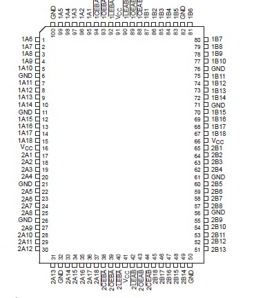
SpecificationsSupply voltage range, VCC . . . . . . . . . . . . . . . . . . . . . . . . . . . . . . . . . . . . . . . . . . . . 0.5 V to 7 V
Input voltage range, VI (except I/O ports) (see Note 1) . . . . . . . . . . . . . . . . . . . . . 0.5 V to 7 V
Voltage range applied to any output in the high or power-off state, VO . . . . . . . 0.5 V to 5.5 V
Current into any output in the low state, IO: SN54ABTH32543 . . . . . . . . . . . . . . . . . . . . . . . 96 mA
SN74ABTH32543 . . . . . . . . . . . . . . . . . . . . . . 128 mA
Input clamp current, IIK (VI < 0) . . . . . . . . . . . . . . . . . . . . . . . . . . . . . . . . . . . . . . . . . . . . . 18 mA
Output clamp current, IOK (VO < 0) . . . . . . . . . . . . . . . . . . . . . . . . . . . . . . . . . . . . . . . . . . 50 mA
Package thermal impedance, JA (see Note 2): PZ package . . . . . . . . . . . . . . . . . . . . . . . . 50°C/W
Storage temperature range, Tstg . . . . . . . . . . . . . . . . . . . . . . . . . . . . . . . . . . . . . 65°C to 150°C
† Stresses beyond those listed under "absolute maximum ratings" may cause permanent damage to the device. These are stress ratings only, and functional operation of the device at these or any other conditions beyond those indicated under "recommended operating conditions" is not implied. Exposure to absolute-maximum-rated conditions for extended periods may affect device reliability.NOTES: 1. The input and output negative-voltage ratings may be exceeded if the input and output clamp-current ratings are observed. 2. The package thermal impedance is calculated in accordance with EIA/JEDEC Std JESD51.
DescriptionThe 'ABTH32543 are 36-bit registered transceivers that contain two sets of D-type latches for temporary storage of data flowing in either direction. These devices can be used as two 18-bit transceivers or one 36-bit transceiver. Separate latch-enable (LEAB or LEBA) and output-enable (OEAB or OEBA) inputs are provided for each register to permit independent control in either direction of data flow.
The A-to-B enable (CEAB) input of 'ABTH32543 must be low to enter data from A or to output data from B. If CEAB is low and LEAB is low, the A-to-B latches are transparent; a subsequent low-to-high transition of LEAB puts the A latches in the storage mode. With CEAB and OEAB both low, the 3-state B outputs are active and reflect the data present at the output of the A latches. Data flow from B to A is similar but requires using the CEBA,LEBA, and OEBA inputs.

 SN74ABTH32543 Data Sheet


