Features: · EPICETM (Enhanced-Performance Implanted CMOS) Process
· Inputs Are TTL-Voltage Compatible
· Latch-Up Performance Exceeds 250 mA Per JESD 17
· ESD Protection Exceeds 2000 V Per MIL-STD-883, Method 3015; Exceeds 200 V Using Machine Model (C = 200 pF, R = 0)
· Package Options Include Plastic Small-Outline Transistor (DBV, DCK) Packages
Pinout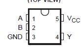 Specifications
Supply voltage range, VCC . . . . . . . . . . . . . . . . . . . . . . . . . . . 0.5 V to 7 V
Input voltage range, VI (see Note 1) . . . . . . . . . . . . . . . . . . . 0.5 V to 7 V
Output voltage range, VO (see Note 1) . . . . . . . . . . . 0.5 V to VCC + 0.5 V
Input clamp current, IIK (VI < 0) . . . . . . . . . . . . . . . . . . . . . .. . . . . . 20 mA
Output clamp current, IOK (VO < 0 or VO > VCC) . . . . . . . . . . . . . . . ±20 mA
Continuous output current, IO (VO = 0 to VCC) . . . . . . . .. . . . . . . . . ±25 mA
Continuous current through VCC or GND . . . . . . . . . . . . . . . . .. . . . . ±50 mA
Package thermal impedance, JA (see Note 2): DBV package . . . . 347°C/W
DCK package . .. . . 389°C/W
Storage temperature range, Tstg . . . . . . . . . . . . . . . . . . . 65°C to 150°C
† Stresses beyond those listed under "absolute maximum ratings" may cause permanent damage to the device. These are stress ratings only, and functional operation of the device at these or any other conditions beyond those indicated under "recommended operating conditions" is not implied. Exposure to absolute-maximum-rated conditions for extended periods may affect device reliability.
NOTES: 1. The input and output voltage ratings may be exceeded if the input and output current ratings are bserved.
2. The package thermal impedance is calculated in accordance with JESD 51.
DescriptionThis device contains a single 2-input NOR gate that performs the Boolean function Y = A• B or Y = A + B in positive logic.The SN74AHCT1G02 is characterized for operation from 40°C to 85°C.

 SN74AHCT1G02 Data Sheet


