SN74AHCT367DR

Buffers & Line Drivers Tri-State Hex

product image

SN74AHCT367DR Picture
SeekIC No. : 00404707 Detail

SN74AHCT367DR: Buffers & Line Drivers Tri-State Hex

floor Price/Ceiling Price

US $ .18~.39 / Piece | Get Latest Price
Part Number:
SN74AHCT367DR
Mfg:
Texas Instruments
Supply Ability:
5000

Price Break

  • Qty
  • 0~1
  • 1~25
  • 25~100
  • 100~250
  • Unit Price
  • $.39
  • $.24
  • $.21
  • $.18
  • Processing time
  • 15 Days
  • 15 Days
  • 15 Days
  • 15 Days
View more price & deliveries
Total Cost: $ 0.00

SeekIC Buyer Protection PLUS - newly updated for 2013!

  • Escrow Protection.
  • Guaranteed refunds.
  • Secure payments.
  • Learn more >>

Month Sales

268 Transactions

Rating

evaluate  (4.8 stars)

Upload time: 2025/12/24

Payment Methods

All payment methods are secure and covered by SeekIC Buyer Protection PLUS.

Notice: When you place an order, your payment is made to SeekIC and not to your seller. SeekIC only pays the seller after confirming you have received your order. We will also never share your payment details with your seller.
Product Details

Quick Details

Number of Input Lines : 6 Number of Output Lines : 6
Polarity : Non-Inverting Supply Voltage - Max : 5.5 V
Supply Voltage - Min : 4.5 V Maximum Operating Temperature : + 85 C
Mounting Style : SMD/SMT Package / Case : SOIC-16
Packaging : Reel    

Description

Number of Input Lines : 6
Number of Output Lines : 6
Polarity : Non-Inverting
Maximum Operating Temperature : + 85 C
Mounting Style : SMD/SMT
Packaging : Reel
Supply Voltage - Max : 5.5 V
Supply Voltage - Min : 4.5 V
Package / Case : SOIC-16


Features:

` Inputs Are TTL-Voltage Compatible
` True Outputs
` Latch-Up Performance Exceeds 100 mA Per
  JESD 78, Class II
` ESD Protection Exceeds JESD 22
2000-V Human-Body Model (A114-A)
200-V Machine Model (A115-A)
1000-V Charged-Device Model (C101)


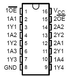
Pinout

  Connection Diagram


Specifications

Supply voltage range, VCC . . . . . . . . . . . . . . . . . . . . . . . . . . . . . . . . . . . . . . . . . . . . . . . . .0.5 V to 7 V
Input voltage range, VI (see Note 1) . . . . . . . . . . . . . . . . . . . . . . . . . . . . . . . . . . . . . . . . . 0.5 V to 7 V
Output voltage range, VO (see Note 1) . . . . . . . . . . . . . . . . . . . . . . . . . . . . . . . . .0.5 V to VCC + 0.5 V
Input clamp current, IIK (VI < 0) . . . . . . . . . . . . . . . . . . . . . . . . . . . . . . . . . . . . . . . . . . . . . . . . . 20 mA
Output clamp current, IOK (VO < 0 or VO > VCC) . . . . . . . . . . . . . . . . . . . . . . . . . . . . . . . . . . . . .±20 mA
Continuous output current, IO (VO = 0 to VCC) . . . . . . . . . . . . . . . . . . . . . . . . . . . . . . . . . . . . . . ±25 mA
Continuous current through VCC or GND . . . . . . . . . . . . . . . . . . . . . . . . . . . . . . . . . . . . . . . . . . . ±75 mA
Package thermal impedance, JA (see Note 2): D package . . . . . . . . . . . . . . . . . . . . . . . . . . . . . 73°C/W
DB package . . . . . . . . . . . . . . . . . . . . . . . . . . . . . . . . .  . . . . . . . . . . . . . . . . . . . . . . . . . . . . . . . . 82°C/W
DGV package . . . . . . . . . . . . . . . . . . . . . . . . . . . . . . .  . . . . . . . . . . . . . . . . . . . . . . . . . . . . . . . . 120°C/W
N package . . . . . . . . . . . . . . . . . . . . . . . . . . . . . . . . . . .  . . . . . . . . . . . . . . . . . . . . . . . . . . . . . . . 67°C/W
NS package . . . . . . . . . . . . . . . . . . . . . . . . . . . . . . . . .  . . . . . . . . . . . . . . . . . . . . . . . . . . . . . . . .  64°C/W
PW package . . . . . . . . . . . . . . . . . . . . . . . . . . . . . . . .  . . . . . . . . . . . . . . . . . . . . . . . . . . . . . . . . 108°C/W
Storage temperature range, Tstg . . . . . . . . . . . . . . . . . . . . . . . . . . . . . . . . . . . . . . . . . . . 65°C to 150°C
† Stresses beyond those listed under "absolute maximum ratings" may cause permanent damage to the device. These are stress ratings only, and
functional operation of the device at these or any other conditions beyond those indicated under "recommended operating conditions" is not
implied. Exposure to absolute-maximum-rated conditions for extended periods may affect device reliability.
NOTES: 1. The input and output voltage ratings may be exceeded if the input and output current ratings are observed.
2. The package thermal impedance is calculated in accordance with JESD 51-7.


Description

The 'AHCT367 devices are designed specifically to improve both the performance and density of 3-state memory address drivers, clock drivers, and bus-oriented receivers and transmitters. These devices are organized as dual 4-line and 2-line buffers/drivers with active-low output-enable (1OE and 2OE) inputs. When OE is low, the device passes noninverted data from the A inputs to the Y outputs. When OE is high, the outputs are in the high-impedance state.

To ensure the high-impedance state of 'AHCT367 during power up or power down, OE should be tied to VCC through a pullup resistor; the minimum value of the resistor is determined by the current-sinking capability of the driver.


Parameters:

Technical/Catalog InformationSN74AHCT367DR
VendorTexas Instruments (VA)
CategoryIntegrated Circuits (ICs)
Logic TypeLine Driver, Non-Inverting
Package / Case16-SOIC (3.9mm Width)
PackagingCut Tape (CT)
Mounting TypeSurface Mount
Number of Bits per Element2, 4
Number of Elements2 - Dual
Operating Temperature-40°C ~ 85°C
Voltage - Supply4.5 V ~ 5.5 V
Current - Output High, Low8mA, 8mA
Drawing Number296; 4040047-4; D; 16
Lead Free StatusLead Free
RoHS StatusRoHS Compliant
Other Names SN74AHCT367DR
SN74AHCT367DR
296 4735 1 ND
29647351ND
296-4735-1


Customers Who Bought This Item Also Bought

Margin,quality,low-cost products with low minimum orders. Secure your online payments with SeekIC Buyer Protection.
Optoelectronics
Transformers
Optical Inspection Equipment
Crystals and Oscillators
Memory Cards, Modules
View more