Features: Operates From 1.65 V to 3.6 V Max tpd of 3.4 ns at 3.3 V ±24-mA Output Drive at 3.3 V Latch-Up Performance Exceeds 250 mA Per JESD 17PinoutSpecificationsSupply voltage range, VCC . . . . . . . . . . . . . .. . . . . . . . . . .. ........ . . −0.5 V to 4.6 VInput voltage range, VI: ...
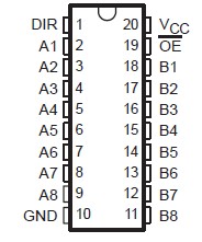
SN74ALVC245: Features: Operates From 1.65 V to 3.6 V Max tpd of 3.4 ns at 3.3 V ±24-mA Output Drive at 3.3 V Latch-Up Performance Exceeds 250 mA Per JESD 17PinoutSpecificationsSupply voltage range, VCC . . . . ....
SeekIC Buyer Protection PLUS - newly updated for 2013!
268 Transactions
All payment methods are secure and covered by SeekIC Buyer Protection PLUS.

Supply voltage range, VCC . . . . . . . . . . . . . .. . . . . . . . . . .. ........ . . −0.5 V to 4.6 V
Input voltage range, VI: Except I/O ports (see Note 1) . ....... .. ... . −0.5 V to 4.6 V
I/O ports (see Notes 1 and 2) . ......−0.5 V to VCC + 0.5 V
Output voltage range, VO (see Notes 1 and 2) . . .. . ....... . ..−0.5 V to VCC + 0.5 V
Input clamp current, IIK (VI < 0) . . . . . . . . . . . . . . . ....... . . ......... . . . . . . . −50 mA
Output clamp current, IOK (VO < 0) . . . . . . . . . . . . . . ....... . . . . . .. . . . . . . −50 mA
Continuous output current, IO . . . . . . . . . . . . . . . . . . . . ....... . . . . .. . . . . . ±50 mA
Continuous current through VCC or GND . . . . . . . . . . ..... . ....... . . . .. . . . ±100 mA
Package thermal impedance, JA (see Note 3): DGV package ....... . .. . . . . 92°C/W
(see Note 3): DW package. . . ....... .. . . . 58°C/W
(see Note 3): NS package .. . ....... . . . . . 60°C/W
(see Note 3): PW package . . ....... . . . . . 83°C/W
(see Note 4): RGY package . ....... . . . . .. 37°C/W
Storage temperature range, Tstg . . . . . . ........................... . . . . . −65°C to 150°C
† Stresses beyond those listed under "absolute maximum ratings" may cause permanent damage to the device. These are stress ratings only, and functional operation of the device at these or any other conditions beyond those indicated under "recommended operating conditions" is not implied. Exposure to absolute-maximum-rated conditions for extended periods may affect device reliability.
NOTES: 1. The input negative-voltage and output voltage ratings may be exceeded if the input and output current ratings are observed.
2. This value is limited to 4.6 V maximum.
3. The package thermal impedance is calculated in accordance with JESD 51-7.
4. The package thermal impedance is calculated in accordance with JESD 51-5.
This SN74ALVC245 octal bus transceiver is designed for 1.65-V to 3.6-V VCC operation.
The SN74ALVC245 is designed for asynchronous communication between data buses. The device transmits data from the A bus to the B bus or from the B bus to the A bus, depending on the logic level at the direction-control (DIR) input. The output-enable (OE) input can be used to disable the device so the buses are effectively isolated.
To ensure the high-impedance state of SN74ALVC245 during power up or power down, OE should be tied to VCC through a pullup resistor; the minimum value of the resistor is determined by the current-sinking capability of the driver.