Features: · Member of the Texas Instruments Widebus™ Family· Ideal for Use in PC133 Register DIMM· Typical Output Skew . . . <250 ps· VCC = 3.3 V ± 0.3 V . . . Normal Range· VCC = 2.7 V to 3.6 V . . . Extended Range· VCC = 2.5 V ± 0.2 V· Rail-to-Rail Output Swing for Increased Noise Margi...
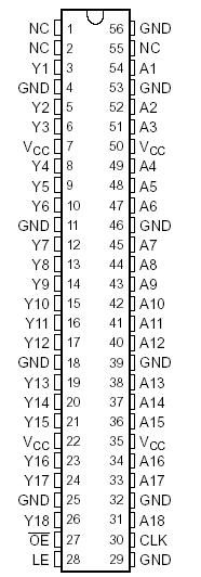
SN74ALVCF162835: Features: · Member of the Texas Instruments Widebus™ Family· Ideal for Use in PC133 Register DIMM· Typical Output Skew . . . <250 ps· VCC = 3.3 V ± 0.3 V . . . Normal Range· VCC = 2.7 V to ...
SeekIC Buyer Protection PLUS - newly updated for 2013!
268 Transactions
All payment methods are secure and covered by SeekIC Buyer Protection PLUS.

|
MIN |
MAX |
UNIT | ||
|
VCC Supply voltage range |
0.5 |
6.5 |
V | |
|
VI Input voltage range(2) |
0.5 |
6.5 |
V | |
|
VO Output voltage range(2) (3) |
0.5 |
VCC + 0.5 |
V | |
|
IIK Input clamp current |
VI < 0 or VI < VCC |
50 |
mA | |
|
IOK Output clamp current |
VO < 0 |
50 |
mA | |
|
IO Continuous output current |
±50 |
mA | ||
|
Continuous current through each VCC or GND |
±100 |
mA | ||
|
JA Package thermal impedance(4) |
DGG package |
40 |
/W | |
| DGV package | ||||
| DL package | ||||
|
Tstg Storage temperature range |
-65 |
150 |
||
This SN74ALVCF162835 18-bit universal bus driver is designed for 2.3-V to 3.6-V VCC operation.
Data of SN74ALVCF162835 flow from A to Y is controlled by the output-enable (OE) input. The device operates in the transparent mode when the latch-enable (LE) input is high. When LE is low, the A data is latched if the clock (CLK) input is held at a high or low logic level. If LE is low, the A data is stored in the latch/flip-flop on the low-to-high transition of CLK. When OE is high, the outputs are in the high-impedance state.
The SN74ALVCF162835 has series damping resistors in the device output structure that reduce switching noise in 128-MB and 256-MB SDRAM modules. Designed with a drive capability of ±18 mA, this device is a midway drive between the SN74ALVC162835 (±12 mA) and SN74ALVC16835 (±24 mA).