Pinout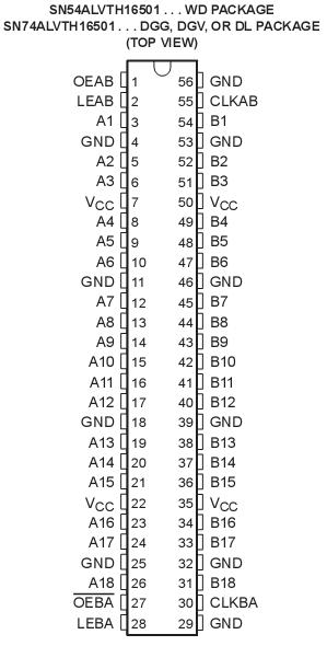 Specifications
Supply voltage range, VCC . . . . . . . . . . . . . . . . . . . . . . . . . . . . . . . . . . . . . . . . . . . . . . . . . . 0.5 V to 4.6 V
Input voltage range, VI (see Note 1) . . . . . . . . . . . . . . . . . . . . . . . . . . . . . . . . . . . . . . . . . . . . 0.5 V to 7 V
Voltage range applied to any output in the high or power-off state, VO (see Note 1) . . . . . . .0.5 V to 7 V
Output current in the low state, IO : SN54ALVTH16501 . . . . . . . . . . . . . . . . . . . . . . . . . . . . . . . . . ... .96 mA
SN74ALVTH16501 . . . . . . . . . . . . . . . . . . . . . . . . . . . . . . . . . ....128 mA
Output current in the high state, IO : SN54ALVTH16501 . . . . . . . . . . . . . . . . . . . . . . . . . . . . . . . . .. . 48 mA
SN74ALVTH16501 . . . . . . . . . . . . . . . . . . . . . . . . . . . . . . . . . . 64 mA
Input clamp current, IIK (V I< 0) . . . . . . . . . . . . . . . . . . . . . . . . . . . . . . . . . . . . . . . . . . . . . . . . . . .. .50 mA
Output clamp current, IOK (VO < 0) . . . . . . . . . . . . . . . . . . . . . . . . . . . . . . . . . . . . . . . . . . . . . . . . . 50 mA
Package thermal impedance, JA (see Note 2): DGG package . . . . . . . . . . . . . . . . . . . . . . . . . . . . . . . 81/W
DGV package . . . . . . . . . . . . . . . . . . . . . . . . . .. 86/W
DL package . . . . . . . . . . . . . . . . . . . . . . . . . . . 74/W
Storage temperature range, Tstg . . . . . . . . . . . . . . . . . . . . . . . . . . . . . . . . . . . . . . . . . . . . . .65 to 150
DescriptionThe SN74ALVTH16501 devices are 18-bit universal bus transceivers designed for 2.5-V or 3.3-V VCC operation, but with the capability to provide a TTL interface to a 5-V system environment.
Data flow in each direction is controlled by output-enable (OEAB and OEBA ), latch-enable (LEAB and LEBA),and clock (CLKAB and CLKBA) inputs. For A-to-B data flow, the devices operate in the transparent mode when LEAB is high. When LEAB is low, the A data is latched if CLKAB is held at a high or low logic level. If LEAB is low, the A data is stored in the latch/flip-flop on the low-to-high transition of CLKAB. When OEAB is high, the B-port outputs are active. When OEAB is low, the B-port outputs are in the high-impedance state.Data flow for B to A is similar to that of A to B but uses OEBA, LEBA, and CLKBA. The output of SN74ALVTH16501 enables are complementary (OEAB is active high and OEBA is active low).
When VCC is between 0 and 1.2 V, the device is in the high-impedance state during power up or power down. However, to ensure the high-impedance state of SN74ALVTH16501 above 1.2 V, OEBAshould be tied to V CC through a pullup resistor and OEAB should be tied to GND through a pulldown resistor; the minimum value of the resistor is determined by the current-sinking/current-sourcing capability of the driver. Active bus-hold circuitry is provided to hold unused or floating data inputs at a valid logic level.
The SN54ALVTH16501 is characterized for operation over the full military temperature range of 55 to 125 . The SN74ALVTH16501 is characterized for operation from 40 to 85 .

 SN74ALVTH16501 Data Sheet


