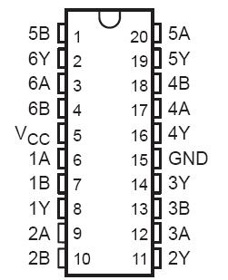
SN74AS1808: Features: • High Capacitive-Drive Capability• Typical Delay Time of 3.2 ns (CL = 50 pF) and Typical Power Dissipation of Less Than 13 mW Per Gate• Center VCC and GND Configuration ...
floor Price/Ceiling Price
- Part Number:
- SN74AS1808
- Supply Ability:
- 5000
Price Break
- Qty
- 1~5000
- Unit Price
- Negotiable
- Processing time
- 15 Days
SeekIC Buyer Protection PLUS - newly updated for 2013!
- Escrow Protection.
- Guaranteed refunds.
- Secure payments.
- Learn more >>
Month Sales
268 Transactions
Payment Methods
All payment methods are secure and covered by SeekIC Buyer Protection PLUS.

 SN74AS1808 Data Sheet


