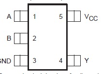
Features: ` Available in the Texas Instruments NanoStar and NanoFree Packages` Low Static Power Consumption; ICC = 0.9 A Max` Low Dynamic Power Consumption; Cpd = 4.3 pF Typ at 3.3 V` Low Input Capacitance; Ci = 1.5 pF Typ` Low Noise; Overshoot and Undershoot <10% of VCC` Ioff S...
SN74AUP1G02: Features: ` Available in the Texas Instruments NanoStar and NanoFree Packages` Low Static Power Consumption; ICC = 0.9 A Max` Low Dynamic Power Consumption; Cpd = 4.3 pF Typ at 3.3 V...
SeekIC Buyer Protection PLUS - newly updated for 2013!
268 Transactions
All payment methods are secure and covered by SeekIC Buyer Protection PLUS.
` Available in the Texas Instruments NanoStar and NanoFree Packages
` Low Static Power Consumption; ICC = 0.9 A Max
` Low Dynamic Power Consumption; Cpd = 4.3 pF Typ at 3.3 V
` Low Input Capacitance; Ci = 1.5 pF Typ
` Low Noise; Overshoot and Undershoot <10% of VCC
` Ioff Supports Partial-Power-Down Mode Operation
` Input Hysteresis Allows Slow Input Transition and Better Switching Noise Immunity at the Input (Vhys = 250 mV Typ at 3.3 V)
` Wide Operating VCC Range of 0.8 V to 3.6 V
` Optimized for 3.3-V Operation
` 3.6-V I/O Tolerant to Support Mixed-Mode Signal Operation
` tpd = 4.5 ns Max at 3.3 V
` Suitable for Point-to-Point Applications
` Latch-Up Performance Exceeds 100 mA Per JESD 78, Class II
` ESD Performance Tested Per JESD 22
− 2000-V Human-Body Model(A114-B, Class II)
− 200-V Machine Model (A115-A)
− 1000-V Charged-Device Model (C101)
`ESD Protection Exce

| Supply voltage range, VCC | −0.5 V to 4.6 V |
| Input voltage range, VI (see Note 1) | −0.5 V to 4.6 V |
| Voltage range applied to any output in the high-impedance or power-off state, VO (see Note 1) | −0.5 V to 4.6 V |
| Output voltage range in the high or low state, VO (see Note 1) | −0.5VtoVCC+0.5V |
| Input clamp current, IIK (VI < 0) | −50 mA |
| Output clamp current, IOK (VO < 0) | −50 mA |
| Continuous output current, IO | ±20 mA |
| Continuous current through VCC or GND | ±50 mA |
| Package thermal impedance, JA (see Note 2): DBV package DCK package DRL package YEP/YZP package |
206/W 252/W 142/W 132/W |
| Storage temperature range, Tstg | −65 to 150 |
NOTES: 1. The input and output negative-voltage ratings may be exceeded if the input and output current ratings are observed.
2. The package thermal impedance is calculated in accordance with JESD 51-7.
The AUP family is TI's premier solution to the industry's low-power needs in battery-powered portable applications. This SN74AUP1G02 family ensures a very low static and dynamic power consumption across the entire VCC range of 0.8 V to 3.6 V, resulting in an increased battery life. This product also maintains excellent signal integrity (see Figures 1 and 2).