Type
:
Supply Current
:
Supply Voltage - Max
: 3.6 V
Maximum Operating Temperature
: + 85 C
Mounting Style
: SMD/SMT
Propagation Delay Time
: 5.5 ns
Supply Voltage - Min
: 2.3 V
Package / Case
: DSBGA-6
Features: · Available in the Texas Instruments
NanoStar and NanoFree Packages
· Single-Supply Voltage Translator
− 1.8 V to 3.3 V (at VCC = 3.3 V)
− 2.5 V to 3.3 V (at VCC = 3.3 V)
− 1.8 V to 2.5 V (at VCC = 2.5 V)
− 3.3 V to 2.5 V (at VCC = 2.5 V)
· Nine Configurable Gate Logic Functions
· Schmitt-Trigger Inputs Reject Input Noise
and Provide Better Output Signal Integrity
· Ioff Supports Partial-Power-Down Mode
With Low Leakage Current (0.5 · A)
· 200-ns/V Input Rise/Fall Time Allows Slow
Transition of Input Signal
· Very Low Static and Dynamic Power Consumption
· Pb-Free Packages Available: SOT-23 (DBV),
SC-70 (DCK), WCSP (NanoFree)
· Latch-Up Performance Exceeds 100 mA Per
JESD 78, Class II
· ESD Performance Tested Per JESD 22
− 2000-V Human-Body Model
(A114-B, Class II)
− 200-V Machine Model (A115-A)
− 1000-V Charged-Device Model (C101)
· Related Devices: AUP1T98/57/58Pinout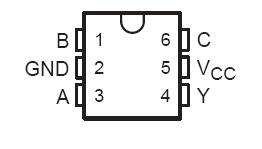 SpecificationsSupply voltage range, VCC . . . . . . . . . . . . . . . . . . . . . . . . . . . . . . . . . . . . . . . . . . . . . . . . . . . .−0.5 V to 4.6 V
Input voltage range, VI (see Note 1) . . . . . . . . . . . . . . . . . . . . . . . . . . . . . . . . . . . . . . . . . . . . −0.5 V to 4.6 V
Voltage range applied to any output in the high-impedance or power-off state, VO
(see Note 1) . . . . . . . . . . . . . . . . . . . . . . . . . . . . . . . . . . . . . . . . . . . . . . . . . . . . . . . . . . . . . . . −0.5 V to 4.6 V
Output voltage range in the high or low state, VO (see Note 1) . . . . . . . . . . . . . . . . . . −0.5 V to VCC + 0.5 V
Input clamp current, IIK (VI < 0) . . . . . . . . . . . . . . . . . . . . . . . . . . . . . . . . . . . . . . . . . . . . . . . . . . . . . . −50 mA
Output clamp current, IOK (VO < 0) . . . . . . . . . . . . . . . . . . . . . . . . . . . . . . . . . . . . . . . . . . . . . . . . . . . .−50 mA
Continuous output current, IO . . . . . . . . . . . . . . . . . . . . . . . . . . . . . . . . . . . . . . . . . . . . . . . . . . . . . . . .±20 mA
Continuous current through VCC or GND . . . . . . . . . . . . . . . . . . . . . . . . . . . . . . . . . . . . . . . . . . . . . . . . ±50 mA
Package thermal impedance, JA (see Note 2): DBV package . . . . . . . . . . . . . . . . . . . . . . . . . . . . . . . 165°C/W
DCK package . . . . . . . . . . . . . . . . . . . . . . . . . . . . . . . . . . . . . . . . . . . . . . . . . . . . . . . . . . . . . . . . . . . . 259°C/W
YEP/YZP package . . . . . . . . . . . . . . . . . . . . . . . . . . . . . . . . . . . . . . . . . . . . . . . . . . . . . . . . . . . . . . . . . 123°C/W
Storage temperature range, Tstg . . . . . . . . . . . . . . . . . . . . . . . . . . . . . . . . . . . . . . . . . . . . . . . −65°C to 150°C
† Stresses beyond those listed under "absolute maximum ratings" may cause permanent damage to the device. These are stress ratings only, and
functional operation of the device at these or any other conditions beyond those indicated under "recommended operating conditions" is not
implied. Exposure to absolute-maximum-rated conditions for extended periods may affect device reliability.
NOTES: 1. The input negative-voltage and output voltage ratings may be exceeded if the input and output current ratings are observed.
2. The package thermal impedance is calculated in accordance with JESD 51-7.DescriptionSN74AUP1T97YEPR AUP technology is the industry's lowest-power logic technology designed for use in battery-operated or battery backed-up equipment. The SN74AUP1T97 is designed for logic level translation applications with input switching levels that accept 1.8-V LVCMOS signals, while operating from either a single 3.3-V or 2.5-V VCC supply.
The wide SN74AUP1T97YEPR VCC range of 2.3 V to 3.6 V allows the possibility of battery voltage drop during system operation and ensures normal operation between this range.
SN74AUP1T97YEPR Schmitt-trigger inputs ( �VT = 210 mV between positive and negative input transitions) offer improved noise immunity during switching transitions, which is especially useful on analog-mixed mode designs. Schmitt-trigger inputs reject input noise, ensure integrity of output signals, and also allow for slow input signal transition. The AUP1T97 can be easily configured to perform a required gate function by connecting A, B, and C inputs to VCC or ground (see Function Selection Table). Up to nine commonly used logic gate functions can be
performed.
SN74AUP1T97YEPR Ioff is a feature that allows for powered-down conditions (VCC = 0 V) and is important in portable and mobile applications. When VCC = 0 V, signals in the range from 0 V to 3.6 V can be applied to the inputs and outputs of the device. No damage will occur to the device under these conditions.
AUP1T97 is designed with optimized current drive capability of 4 mA to reduce line reflections, overshoot, and undershoot caused by high drive outputs.
SN74AUP1T97YEPR Nanostar and Nanofree package technology is a major breakthrough in IC packaging concepts, using the die as the package.
Parameters: | Technical/Catalog Information | SN74AUP1T97YEPR |
| Vendor | Texas Instruments |
| Category | Integrated Circuits (ICs) |
| Package / Case | 6-DSBGA |
| Packaging | Tape & Reel (TR) |
| Input Type | Voltage |
| Output Type | Voltage |
| Supply Voltage | 2.3 V ~ 3.6 V |
| Data Rate | - |
| Number of Channels | - |
| Operating Temperature | -40°C ~ 85°C |
| Drawing Number | 296; 4204725-3; YEP; 6 |
| Lead Free Status | Lead Free |
| RoHS Status | RoHS Compliant |
| Other Names | SN74AUP1T97YEPR
SN74AUP1T97YEPR
|

 SN74AUP1T97YEPR Data Sheet


