Pinout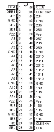 SpecificationsSupply voltage range, VCC . . . . . . . . . . . . . . . . . . . . . . . . . . . . . . . . . . . . . . . . . . . . . . .0.5 V to 4.6 V
Input voltage range, VI (see Note 1) . . . . . . . . . . . . . . . . . . . . . . . . . . . . . . . . . . . . . . . .0.5 V to 4.6 V
Voltage range applied to any input/output when the output
is in the high-impedance or power-off state, VO (see Note 1) . . . . . . . . . . . . . . . . . . 0.5 V to 4.6 V
Voltage range applied to any input/output when the output
is in the high or low state, VO (see Notes 1 and 2) . . . . . . . . . . . . . . . . . . . . . . .0.5 V to VCC + 0.5 V
Input clamp current, IIK (VI < 0) . . . . . . . . . . . . . . . . . . . . . . . . . . . . . . . . . . . . . . . . . . . . . . . . . .50 mA
Output clamp current, IOK (VO < 0) . . . . . . . . . . . . . . . . . . . . . . . . . . . . . . . . . . . . . . . . . . . . . . . .50 mA
Continuous output current, IO . . . . . . . . . . . . . . . . . . . . . . . . . . . . . . . . . . . . . . . . . . . .. . . . . . . .±50 mA
Continuous current through each VCC or GND . . . . . . . . . . . . . . . . . . . . . . . . . .. . . . . . . . . . . . .±100 mA
Package thermal impedance, JA (see Note 3): DGG package . . . . . . . . . . . . . . . . . . . . . . . .. . . .64°C/W
DGV package . . . . . . . . . . . . . . . . . . . . .. . . . . . .48°C/W
Storage temperature range, Tstg . . . . . . . . . . . . . . . . . . . . . . . . . . . . . . . . . . . . . . .. . . . .65°C to 150°C DescriptionA SN74AVC16269 Dynamic Output Control (DOC) circuit is implemented, which, during the transition, initially lowers the output impedance to effectively drive the load and, subsequently, raises the impedance to reduce noise. Figure 1 shows typical VOL vs IOL and VOH vs IOH curves to illustrate the output impedance and drive capability of the circuit. At the beginning of the signal transition, the SN74AVC16269 DOC circuit provides a maximum dynamic drive that is equivalent to a high-drive standard-output device. For more information, refer to the TI application reports, AVC Logic Family Technology and Applications, literature number SCEA006, and Dynamic Output Control (DOCTM) Circuitry Technology and Applications, literature number SCEA009.
This SN74AVC16269 12-bit (dual octal) noninverting bus transceiver is operational at 1.2-V to 3.6-V VCC, but is designed specifically for 1.65-V to 3.6-V VCC operation.
The SN74AVC16269 is used in applications in which two separate ports must be multiplexed onto, or demultiplexed from, a single port. The device is particularly suitable as an interface between synchronous DRAMs and high-speed microprocessors.
Data is stored in the internal B-port registers on the low-to-high transition of the clock (CLK) input when the appropriate clock-enable (CLKENA) inputs are low. Proper control of these inputs allows two sequential 12-bit words to be presented as a 24-bit word on the B port. For SN74AVC16269 data transfer in the B-to-A direction, a single storage register is provided. The select (SEL) line selects 1B or 2B data for the A outputs. The register on the A output permits the fastest possible data transfer, thus extending the period during which the data is valid on the bus.
The control SN74AVC16269 terminals are registered so that all transactions are synchronous with CLK. Data flow is controlled by the active-low output enables (OEA, OEB1, OEB2).
To ensure the SN74AVC16269 high-impedance state during power up or power down, a clock pulse should be applied as soon as possible, andOE should be tied to VCC through a pullup resistor; the minimum value of the resistor is determined by the current-sinking capability of the driver. Due to OE being routed through a register, the active state of the outputs cannot be determined prior to the arrival of the first clock pulse.
This SN74AVC16269 device is fully specified for partial-power-down applications using Ioff. The Ioff circuitry disables the outputs, preventing damaging current backflow through the device when it is powered down.
The SN74AVC16269 is characterized for operation from 40°C to 85°C.

 SN74AVC16269 Data Sheet


