Pinout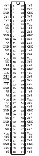 SpecificationsSupply voltage range, VCC . . . . . . . . . . . . . . . . . . . . . . . . . . . . . . . . . . . . . . . . . . . . . . .0.5 V to 4.6 V
Input voltage range, VI (see Note 1) . . . . . . . . . . . . . . . . . . . . . . . . . . . . . . . . . . . . . . . .0.5 V to 4.6 V
Voltage range applied to any output in the high-impedance or power-off state, VO
(see Note 1) . . . . . . . . . . . . . . . . . . . . . . . . . . . . . . . . . . . . . . . . . . . . . . . . . . . . . . . . 0.5 V to 4.6 V
Voltage range applied to any output in the high or low state, VO
(see Notes 1 and 2) . . . . . . . . . . . . . . . . . . . . . . . . . . . . . . . . . . . . . . . . . . . . . .0.5 V to VCC + 0.5 V
Input clamp current, IIK (VI < 0) . . . . . . . . . . . . . . . . . . . . . . . . . . . . . . . . . . . . . . . . . . . . . . . . . .50 mA
Output clamp current, IOK (VO < 0) . . . . . . . . . . . . . . . . . . . . . . . . . . . . . . . . . . . . . . . . . . . . . . . .50 mA
Continuous output current, IO . . . . . . . . . . . . . . . . . . . . . . . . . . . . . . . . . . . . . . . . . . . .. . . . . . . .±50 mA
Continuous current through each VCC or GND . . . . . . . . . . . . . . . . . . . . . . . . . .. . . . . .. . . . . . . .±100 mA
Package thermal impedance, JA (see Note 3): . . . . . . . . . . . . . . . . . . . . . . . . . . . . . . . . . . .. . . .64°C/W
Storage temperature range, Tstg . . . . . . . . . . . . . . . . . . . . . . . . . . . . . . . . . . . . . . . .. . . .65°C to 150°C DescriptionA SN74AVC16831 Dynamic Output Control (DOC) circuit is implemented, which, during the transition, initially lowers the output impedance to effectively drive the load and, subsequently, raises the impedance to reduce noise. Figure 1 shows typical VOL vs IOL and VOH vs IOH curves to illustrate the output impedance and drive capability of the circuit. At the beginning of the signal transition, the DOC circuit provides a maximum dynamic drive that is equivalent to a high-drive standard-output device. For more information, refer to the TI application reports, AVC Logic Family Technology and Applications, literature number SCEA006, and Dynamic Output Control (DOCE) Circuitry Technology and Applications, literature number SCEA009.
This SN74AVC16831 9-bit 1-to-4 address register/driver is operational at 1.2-V to 3.6-V VCC, but is designed specifically for 1.65-V to 3.6-V VCC operation.
The SN74AVC16831 device is ideal for use in applications in which a single address bus is driving four separate memory locations. The SN74AVC16831 can be used as a buffer or a register, depending on the logic level of the select (SEL) input.
When SN74AVC16831 SEL is logic high, the device is in the buffer mode. The outputs follow the inputs and are controlled by the two output-enable (OE) controls. Each OE controls two groups of nine outputs.
When SN74AVC16831 SEL is logic low, the device is in the register mode. The register is an edge-triggered D-type flip-flop. On the positive transition of the clock (CLK) input, data set up at the A inputs is stored in the internal registers. OE controls operate the same as in buffer mode.
When SN74AVC16831 OE is logic low, the outputs are in a normal logic state (high or low logic level). When OE is logic high, the outputs are in the high-impedance state.
SN74AVC16831 SEL and OE do not affect the internal operation of the flip-flops. Old data can be retained or new data can be entered while the outputs are in the high-impedance state.
To ensure the SN74AVC16831 high-impedance state during power up or power down, OE should be tied to VCC through a pullup resistor; the minimum value of the resistor is determined by the current-sinking capability of the driver.
This SN74AVC16831 device is fully specified for partial-power-down applications using Ioff. The Ioff circuitry disables the outputs, preventing damaging current backflow through the device when it is powered down.
The SN74AVC16831 is characterized for operation from 40°C to 85°C.

 SN74AVC16831 Data Sheet


