Features: • High-Bandwidth Data Path (up to 500 MHz (1))
• Equivalent to IDTQS3VH251 Device
• 5-V Tolerant I/Os With Device Powered Up o Powered Down
• Low and Flat ON-State Resistance (r on ) Characteristics Over Operating Range (r on = 4 Ω Typ)
• Rail-to-Rail Switching on Data I/O Ports
0- to 5-V Switching With 3.3-V V CC
0- to 3.3-V Switching With 2.5-V V CC
• Bidirectional Data Flow With Near-Zero Propagation Delay
• Low Input/Output Capacitance Minimizes Loading and Signal Distortion (C io(OFF) = 3.5 pF Typ)
• Fast Switching Frequency (f or f = 20 MHz Max)
• Data and Control Inputs Provide Undershoot
Clamp Diodes
• Low Power Consumption (ICC = 1 mA Typ)
• V CC Operating Range From 2.3 V to 3.6 V
• Data I/Os Support 0- to 5-V Signaling Levels
(0.8 V, 1.2 V, 1.5 V, 1.8 V, 2.5 V, 3.3 V, 5 V)
• Control Inputs Can Be Driven by TTL or 5-V/3.3-V CMOS Outputs
• I off Supports Partial-Power-Down Mode Operation
• Latch-Up Performance Exceeds 100 mA Per JESD 78, Class II
• ESD Performance Tested Per JESD 22
2000-V Human-Body Model (A114-B, Class II)
1000-V Charged-Device Model (C101)
• Supports Both Digital and Analog Applications:
PCI Interface, Differential Signal Interface, Memory Interleaving, Bus Isolation, Low-Distortion Signal Gating
Pinout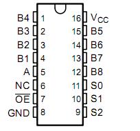 Specifications
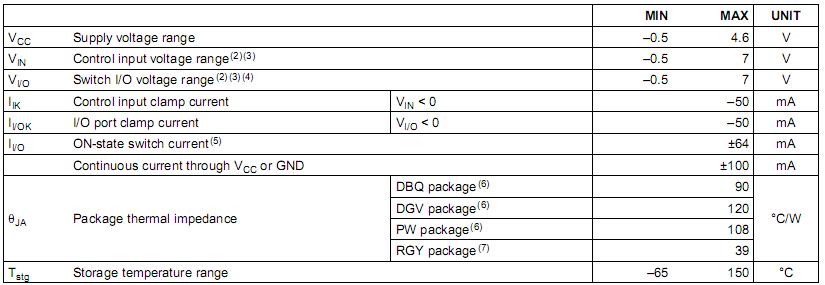
DescriptionThe SN74CB3Q3251 is a high-bandwidth FET bus switch utilizing a charge pump to elevate the gate voltage of the pass transistor, providing a low and flat ON-state resistance (r on ). The low and flat ON-state resistance allows for minimal propagation delay and supports rail-to-rail switching on the data input/output (I/O) ports. The device also features low data I/O capacitance to minimize capacitive loading and signal distortion on the data bus. Specifically designed to support high-bandwidth applications, the SN74CB3Q3251 provides an optimized interface solution ideally suited for broadband communications, networking, and data-intensive computing systems.

 SN74CB3Q3251 Data Sheet


