Pinout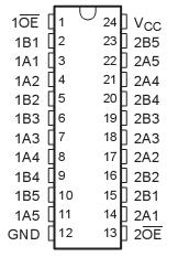 SpecificationsSupply voltage range, VCC . . . . . . . . . . . . . . . . . . . . . . . . . . . . . . . .-0.5 V to 4.6 V
Control input voltage range, VIN(see Notes 1 and 2) . . . . . . . . . . . . -0.5 V to 7 V
Switch I/O voltage range, VI/O(see Notes 1, 2, and 3) . . . . . . . . . . . -0.5 V to 7 V
Control input clamp current, I (V < 0) . . . . . . . . . . . . . . . . . . . . . . . . . . . . -50 mA
IK INON-state switch current, II/O (see Note 4) . . . . . . . . . .. . . . . . . . . ±64 mA
Continuous current through VCC or GND terminals . . . . . . . . . . . . .. . . . ±100 mA
Package thermal impedance, q JA (see Note 5): DBQ package. . . . . . . .. . 61°C/W
DGV package . . . . . . . . . .86°C/W
PW package . . . . . . . . . 88°C/W
Storage temperature range, Tstg . . . . . . . . . . . . . . . .. . . . . . . . . . . .-65 to 150DescriptionThe SN74CB3Q3384A is a high-bandwidth FET bus switch utilizing a charge pump to elevate the gate voltage of the pass transistor, providing a low and flat ON-state resistance (r
on ). The low and flat ON-state resistance allows for minimal propagation delay and supports rail-to-rail switching on the data input/output (I/O) ports. The device also features low data I/O capacitance to minimize capacitive loading and signal distortion on the data bus. Specifically designed to support high-bandwidth applications, the SN74CB3Q3384A provides an optimized interface solution ideally suited for broadband communications, networking, and data-intensive computing systems.
The SN74CB3Q3384A is organized as two 5-bit bus switches with separate output-enable (1OE, 2OE) inputs.It can be used as two 5-bit bus switches, or as one 10-bit bus switch. When OE is low, the associated 5-bit bus switch is ON, and the A port is connected to the B port, allowing bidirectional data flow between ports. When OE is high, the associated 5-bit bus switch is OFF, and a high-impedance state exists between the A and B ports.

 SN74CB3Q3384A Data Sheet


