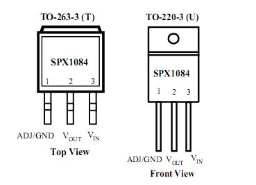
Pinout SpecificationsSupply voltage range, VCC . . . . . . . . . . . . . . . . . . . . . . . . . −0.5 V to 7 V
Control input voltage range, VIN (see Notes 1 and 2) . . . . −0.5 V to 7 V
Switch I/O voltage range, VI/O (see Notes 1, 2, and 3) . . . −0.5 V to 7 V
Control input clamp current, IIK (VIN < 0) . . . . . . . . . . . . . . . . . .−50 mA
I/O port clamp current, II/OK (VI/O < 0) . . . . . . . . . . . . . . . . . . . −50 mA
ON-state switch current, II/O (see Note 4) . . . . . . . . . . . . . . . .±128 mA
Continuous current through VCC or GND terminals . . . . . . . . . ±100 mA
Package thermal impedance, JA (see Note 5): DGG package . . 70°C/W
DGV package . . . . . . . . . . . . . . . . . . . . . . . . . . . . . . . . . . . . . . 58°C/W
DL package . . . . . . . . . . . . . . . . . . . . . . . . . . . . . . . . . .. . . . .. .63°C/W
Storage temperature range, Tstg . . . . . . . . . . . . . . . .−65°C to 150°CDescriptionThe SN74CBT16210C is a high-speed TTL-compatible FET bus switch with low ON-state resistance (ron), allowing for minimal propagation delay. Active Undershoot-Protection Circuitry on the A and B ports of the SN74CBT16210C provides protection for undershoot up to −2 V by sensing an undershoot event and ensuring that the switch remains in the proper OFF state.
The SN74CBT16210C is organized as two 10-bit bus switches with separate output-enable (1OE, 2OE) inputs. It can be used as two 10-bit bus switches or as one 20-bit bus switch. When OE is low, the associated 10-bit bus switch is ON, and the A port is connected to the B port, allowing bidirectional data flow between ports. When OE is high, the associated 10-bit bus switch is OFF, and the high-impedance state exists between the A and B ports.
This SN74CBT162 device is fully specified for partial-power-down applications using Ioff. The Ioff feature ensures that damaging current will not backflow through the device when it is powered down. The device has isolation during power off.
To ensure the SN74CBT162 high-impedance state during power up or power down, OE should be tied to VCC through a pullup resistor; the minimum value of the resistor is determined by the current-sinking capability of the driver.

 SN74CBT162 Data Sheet


