Features: 5- Switch Connection Between Two Ports
Rail-to-Rail Switching on Data I/O Ports
Ioff Supports Partial-Power-Down Mode Operation
Latch-Up Performance Exceeds 250 mA Per JESD 17
ESD Protection Exceeds JESD 22
− 2000-V Human-Body Model (A114-A)
− 200-V Machine Model (A115-A)Pinout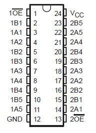 SpecificationsSupply voltage range, VCC . . . . . . . . . . . . . . . . . . . . . . . . . . . . . . . . . . . . . . . . . . . . . . . . . . . . . . . . . −0.5 V to 4.6 V
Input voltage range, VI (see Note 1) . . . . . . . . . . . . . . . . . . . . . . . . . . . . . . . . . . . . . . . . . . . . . . . . . −0.5 V to 4.6 V
Continuous channel current . . . . . . . . . . . . . . . . . . . . . . . . . . . . . . . . . . . . . . . . . . . . . . . . . . . . . . . . . . . . . . 128 mA
Input clamp current, IIK (VI/O < 0) . . . . . . . . . . . . . . . . . . . . . . . . . . . . . . . . . . . . . . . . . . . . . . . . . . . . . . . . . −50 mA
Package thermal impedance, JA (see Note 2): DBQ package . . . . . . . . . . . . . . . . . . . . . . . . . . . . . . . . 61°C/W
DGV package . . . . . . . . . . . . . . . . . . . . . . . . . . . . . . . . 86°C/W
DW package . . . . . . . . . . . . . . . . . . . . . . . . . . . . . . . . . 46°C/W
PW package . . . . . . . . . . . . . . . . . . . . . . . . . . . . . . . . . 88°C/W
Storage temperature range, Tstg . . . . . . . . . . . . . . . . . . . . . . . . . . . . . . . . . . . . . . . . . . . . . . . . . . . −65°C to 150°C
† Stresses beyond those listed under "absolute maximum ratings" may cause permanent damage to the device. These are stress ratings only, and functional operation of the device at these or any other conditions beyond those indicated under "recommended operating conditions" is not implied. Exposure to absolute-maximum-rated conditions for extended periods may affect device reliability.
NOTES: 1. The input and output negative-voltage ratings may be exceeded if the input and output clamp-current ratings are observed.
2. The package thermal impedance is calculated in accordance with JESD 51-7.DescriptionThe SN74CBTLV3384 provides ten bits of high-speed bus switching. The low on-state resistance of the switch allows connections to be made with minimal propagation delay.
The SN74CBTLV3384 is organized as dual 5-bit bus switches with separate output-enable (OE) inputs. It can be used as two 5-bit bus switches or one 10-bit bus switch. When OE is low, the associated 5-bit bus switch is on, and A port is connected to B port. When OE is high, the switch is open, and the high-impedance state exists between the two ports.
This SN74CBTLV3384 is fully specified for partial-power-down applications using I
off. The I
off feature ensures that damaging current will not backflow through the device when it is powered down. The device has isolation during power off.
To ensure the high-impedance state during power up or power down, OE shall be tied to V
CC through a pullup resistor; the minimum value of the resistor is determined by the current-sinking capability of the driver.

 SN74CBTLV3384 Data Sheet


