SN74FB2032

Features: *Compatible With IEEE 1194.1-1991 (BTL) *TTL A Port, Backplane Transceiver Logic (BTL) B Port*Open-Collector B-Port Outputs Sink100 mA*BIAS VCC Minimizes Signal Distortion During Live Insertion or Withdrawal*High-Impedance State During Power Up and Power Down*B-Port Biasing Network Preco...

product image

SN74FB2032 Picture
SeekIC No. : 004498855 Detail

SN74FB2032: Features: *Compatible With IEEE 1194.1-1991 (BTL) *TTL A Port, Backplane Transceiver Logic (BTL) B Port*Open-Collector B-Port Outputs Sink100 mA*BIAS VCC Minimizes Signal Distortion During Live Inse...

floor Price/Ceiling Price

Part Number:
SN74FB2032
Supply Ability:
5000

Price Break

  • Qty
  • 1~5000
  • Unit Price
  • Negotiable
  • Processing time
  • 15 Days
Total Cost: $ 0.00

SeekIC Buyer Protection PLUS - newly updated for 2013!

  • Escrow Protection.
  • Guaranteed refunds.
  • Secure payments.
  • Learn more >>

Month Sales

268 Transactions

Rating

evaluate  (4.8 stars)

Upload time: 2025/12/24

Payment Methods

All payment methods are secure and covered by SeekIC Buyer Protection PLUS.

Notice: When you place an order, your payment is made to SeekIC and not to your seller. SeekIC only pays the seller after confirming you have received your order. We will also never share your payment details with your seller.
Product Details

Description


Features:

*Compatible With IEEE 1194.1-1991 (BTL)
*TTL A Port, Backplane Transceiver Logic (BTL) B Port
*Open-Collector B-Port Outputs Sink100 mA
*BIAS VCC Minimizes Signal Distortion
  During Live Insertion or Withdrawal

*High-Impedance State During Power Up
  and Power Down

*B-Port Biasing Network Preconditions the
  Connector and PC Trace to the BTL
  High-Level Voltage
*TTL-Input Structures Incorporate Active
  Clamping Networks to Aid in Line Termination
*Packaged in Plastic Quad Flatpack


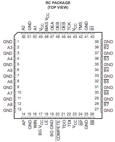
Pinout

  Connection Diagram


Specifications

Supply voltage range, VCC .............................................-0.5 V to 7V 
Input voltage range, VI:Except BP,B port........................-1.2 V to 7V
                                      BP,B port.................................-1.2 V to 3.5V

Voltage range applied to any B output in the disabled
   or power-off state,VO................................................-0.5 V to 3.5V
Voltage range applied to any output in the high state,
                                            VO : A port..........................-0.5 V to VCC

Input clamp current, IIK:Except B port......................................-40mA
                                      B port .................................................-18mA
Current applied to any single output in the low state, IO:
                                      A port...................................................48mA
                                      B port .................................................200mA
Package thermal impedance,  JA(see Note 1).........................44/W
Storage temperature range, Tstg..................................-65 to 150


Description

    The SN74FB2032 device is a 9-bit transceiver designed to translate signals between TTL and backplane transceiver logic (BTL) environments and to perform bus arbitration. It is designed specifically to be compatible with IEEE Std 1194.1-1991.

    The SN74FB2032 B port operates at BTL-signal levels. The open-collector B ports are specified to sink 100 mA and have minimum output edge rates of 2 ns. Two output enables (OEB and OEB) are provided for the B outputs. When OEB is low, OEB is high, or VCC is less than 2.1 V, the B port is turned off.

    The SN74FB2032 A port operates at TTL-signal levels. The A outputs reflect the inverse of the data at the B port when the A-port output enable, OEA, is high. When OEA is low or when VCC is less than 2.1 V, the A outputs are in the high-impedance state.

    The SN74FB2032 A-port data is latched when the latch enable (LE) is high. When LE is low, the latches are transparent.

    The Futurebus protocol logic can be activated by taking COMPETE low. The module (device) then compares SN74FB2032 A data (arbitration number) against the A data of another identical module also connected to the B arbitration bus, and sets WIN high if the A data is greater than the A data of the other module (i.e., has higher priority). A8 and B8 are the most-significant bits, and A1 and B1 are the least-significant bits. If OEB is high and OEB is low during this operation, and the A bus of the first module wins priority, the A bus asserts its arbitration number on the B-arbitration bus.

    AP and BP are the bus-parity bits. The winning module SN74FB2032 can assert BP low if its parity bit (AP) is high.

    In a typical operating sequence, a Futurebus arbitration controller latches its arbitration number into the A port and waits for the results of a competition. When the competition is complete, and if the controller's arbitration number did not win, the controller reads back the current value of the B bus (by taking OEA high) and determines the winning arbitration number. SN74FB2032 allows the module to change its arbitration number for the next competition cycle, if desired.

    Pins are allocated for the four-wire IEEE Std 1149.1 (JTAG) test bus. TMS and TCK are not connected and TDI is shorted to TDO.

    BIAS VCC establishes a voltage between 1.62 V and 2.1 V on the BTL outputs when VCC is not connected. BG VCC and BG GND are the supply inputs for the bias generator.

    The SN74FB2032 is characterized for operation from 0°C to 70°C.


Customers Who Bought This Item Also Bought

Margin,quality,low-cost products with low minimum orders. Secure your online payments with SeekIC Buyer Protection.
Boxes, Enclosures, Racks
Static Control, ESD, Clean Room Products
Crystals and Oscillators
RF and RFID
Optical Inspection Equipment
Industrial Controls, Meters
View more