Features: Member of the Texas Instruments WidebusTM Family
TI-OPCTM Circuitry Limits Ringing on Unevenly Loaded Backplanes
OECTM Circuitry Improves Signal Integrity and Reduces Electromagnetic Interference
Bidirectional Interface Between GTLP Signal Levels and LVTTL Logic Levels
Split LVTTL Port Provides a Feedback Path for Control and Diagnostics Monitoring
LVTTL Interfaces Are 5-V Tolerant High-Drive GTLP Open-Drain Outputs (100 mA)
LVTTL Outputs (24 mA/24 mA)
Variable Edge-Rate Control (ERC) Input Selects GTLP Rise and Fall Times for Optimal Data-Transfer Rate and Signal Integrity in Distributed Loads
Ioff, Power-Up 3-State, and BIAS VCC Support Live Insertion
Distributed VCC and GND Pins Minimize High-Speed Switching Noise
Latch-Up Performance Exceeds 100 mA Per JESD 78, Class II
ESD Protection Exceeds JESD 22
2000-V Human-Body Model (A114-A)
1000-V Charged-Device Model (C101)
Pinout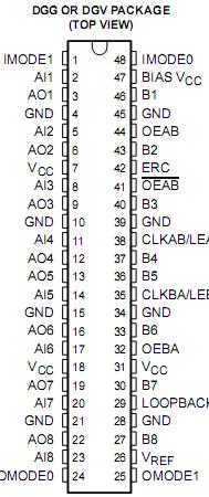 SpecificationsSupply voltage range, VCC and BIAS VCC . . . . . . . . . . . . . . . . . . . . . . . . . . . . . . . .0.5 V to 4.6 V
Input voltage range, VI (see Note 1): AI port, ERC, and control inputs . . . . . . . . . . .0.5 V to 7 V
B port and VREF . . . . . . . . . . . . . . . . . . . . . . . .0.5 V to 4.6 V
Voltage range applied to any output in the high-impedance or power-off state, VO
(see Note 1): AO port . . . . . . . . . . . . . . . . . . . . . . . . . . . . . . . . . . . . . . . . . . . . . . . . ..0.5 V to 7 V
B port . . . . . . . . . . . . . . . . . . . . . . . . . . . . . . . . . . . . . . . . . . . . . . . . . . . . . . . . . . . . .0.5 V to 4.6 V
Current into any output in the low state, IO: AO port . . . . . . . . . . . . . . . . . . . . . . . . . .48 mA
B port . . . . . . . . . . . . . . . . . . . . . . . . . . . . . . . . . . . . . . . . . . .200 mA
Current into any A-port output in the high state, IO (see Note 2) . . . . . . . . . . . . . . . . . . . . .. .48 mA
Continuous current through each VCC or GND . . . . . . . . . . . . . . . . . . . . . . . . . . . . . . . . . .. .±100 mA
Input clamp current, IIK (VI < 0). . . . . . . . . . . . . . . . . . . . . . . . . . . . . . . . . . . . . . . . . . . . . 50 mA
Output clamp current, IOK (VO < 0) . . . . . . . . . . . . . . . . . . . . . . . . . . . . . . . . . . . . . . . . . . . . .50 mA
Package thermal impedance, JA (see Note 3): DGG package . . . . . . . . . . . . . . . . . . . . . .70°C/W
DGV package . . . . . . . . . . . . . . . . . . . . . . .58°C/W
GQL package . . . . . . . . . . . . . . . . . . . . . . . . .42°C/W
Storage temperature range, Tstg . . . . . . . . . . . . . . . . . . . . . . . . . . . . . . . . . . . . . . . .65°C to 150°CDescription The SN74GTLP2033 is a high-drive, 8-bit, three-wire registered transceiver that provides inverted LVTTL-to-GTLP and GTLP-to-LVTTL signal-level translation. The SN74GTLP2033 device allows for transparent, latched, and flip-flop modes of data transfer with separate LVTTL input and LVTTL output pins, which provides a feedback path for control and diagnostics monitoring, the same functionality as the SN74FB2033. The SN74GTLP2033 device provides a high-speed interface between cards operating at LVTTL logic levels and a backplane operating at GTLP signal levels. High-speed (about three times faster than standard LVTTL or TTL) backplane operation is a direct result of GTLP's reduced output swing (<1 V), reduced input threshold levels, improved differential input, OEC
TMcircuitry, and TI-OPC
TM circuitry. Improved GTLP OEC and TI-OPC circuits minimize bus-settling time and have been designed and tested using several backplane models. The high drive allows incident-wave switching in heavily loaded backplanes with equivalent load impedance down to 11 Ω.
GTLP is the Texas Instruments derivative of the Gunning Transceiver Logic (GTL) JEDEC standard JESD 8-3. The ac specification of the SN74GTLP2033 is given only at the preferred higher noise-margin GTLP, but the user has the flexibility of using this SN74GTLP2033 device at either GTL (V
TT = 1.2 V and V
REF = 0.8 V) or GTLP (V
TT = 1.5 V and V
REF = 1 V) signal levels. For information on using GTLP devices in FB+/BTL applications, refer to TI application reports, Texas Instruments GTLP Frequently Asked Questions, literature number SCEA019, and GTLP in BTL Applications, literature number SCEA017.
Normally, the SN74GTLP2033 B port operates at GTLP signal levels. The A-port and control inputs operate at LVTTL logic levels, but are 5-V tolerant and can be directly driven by TTL or 5-V CMOS devices. V
REF is the B-port differential input reference voltage.
This SN74GTLP2033 device is fully specified for live-insertion applications using Ioff, power-up 3-state, and BIAS V
CC. The Ioff circuitry disables the outputs, preventing damaging current backflow through the device when it is powered down. The power-up 3-state circuitry places the outputs in the high-impedance state during power up and power down, which prevents driver conflict. The BIAS VCC circuitry precharges and preconditions the B-port input/output connections, preventing disturbance of active data on the backplane during card insertion or removal, and permits true live-insertion capability.
This GTLP device features TI-OPC circuitry, which actively limits overshoot caused by improperly terminated backplanes, unevenly distributed cards, or empty slots during low-to-high signal transitions. This improves signal integrity, which allows adequate noise margin to be maintained at higher frequencies.
High-drive GTLP backplane interface devices feature adjustable edge-rate control (ERC). Changing the ERC input voltage between low and high adjusts the B-port output rise and fall times. This allows the designer to optimize system data-transfer rate and signal integrity to the backplane load.
When V
CC is between 0 and 1.5 V, the device is in the high-impedance state during power up or power down. However, to ensure the high-impedance state above 1.5 V, OEAB should be tied to V
CC through a pullup resistor and OEAB and OEBA should be tied to GND through a pulldown resistor; the minimum value of the resistor is
determined by the current-sinking/current-sourcing capability of the driver.

 SN74GTLP2033 Data Sheet


