SN74LV245AT

Features: ` Inputs Are TTL-Voltage Compatible ` Ioff Supports Partial-Power-Down Mode Operation` 4.5-V to 5.5-V VCC Operation Operation` Typical tpd of 3.5 ns at 5 V ` Latch-Up Performance Exceeds 250 mA Per JESD 17` Typical VOLP (Output Ground Bounce) <0.8 V at VCC = 5 V, TA = 25°C ` ESD Prote...

product image

SN74LV245AT Picture
SeekIC No. : 004499161 Detail

SN74LV245AT: Features: ` Inputs Are TTL-Voltage Compatible ` Ioff Supports Partial-Power-Down Mode Operation` 4.5-V to 5.5-V VCC Operation Operation` Typical tpd of 3.5 ns at 5 V ` Latch-Up Performance Exceeds 2...

floor Price/Ceiling Price

Part Number:
SN74LV245AT
Supply Ability:
5000

Price Break

  • Qty
  • 1~5000
  • Unit Price
  • Negotiable
  • Processing time
  • 15 Days
Total Cost: $ 0.00

SeekIC Buyer Protection PLUS - newly updated for 2013!

  • Escrow Protection.
  • Guaranteed refunds.
  • Secure payments.
  • Learn more >>

Month Sales

268 Transactions

Rating

evaluate  (4.8 stars)

Upload time: 2025/12/30

Payment Methods

All payment methods are secure and covered by SeekIC Buyer Protection PLUS.

Notice: When you place an order, your payment is made to SeekIC and not to your seller. SeekIC only pays the seller after confirming you have received your order. We will also never share your payment details with your seller.
Product Details

Description


Features:

` Inputs Are TTL-Voltage Compatible
` Ioff Supports Partial-Power-Down Mode Operation
` 4.5-V to 5.5-V VCC Operation Operation
` Typical tpd of 3.5 ns at 5 V
` Latch-Up Performance Exceeds 250 mA Per JESD 17
` Typical VOLP (Output Ground Bounce) <0.8 V at VCC = 5 V, TA = 25°C
` ESD Protection Exceeds JESD 22
2000-V Human-Body Model (A114-A)
1000-V Charged-Device Model (C101)

` Typical VOHV (Output VOH Undershoot) >2.3 V at VCC = 5 V, TA = 25°C


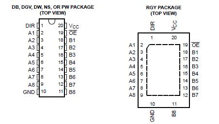
Pinout

  Connection Diagram


Specifications

  MIN MAX UNIT
VCC Supply voltage range 0.5 7 V
VI Input voltage range(2) 0.5 7 V
VO Voltage range applied to any output in the high-impedance or power-off state(2) 0.5 7 V
VO Output voltage range applied in the high or low state(2) (3) 0.5 VCC + 0.5 V
IIK Input clamp current VI < 0   20 mA
IOK Output clamp current VO < 0 or VO > VCC   ±50 mA
IO Continuous output current VO = 0 to VCC   ±35 mA
Continuous current through VCC or GND   ±70 mA
JA Package thermal impedance DB package(4)   70 °C/W
DGV package(4)   92
DW package(4)   58
NS package(4)   60
PW package(4)   83
RGY package(5)   37
Tstg Storage temperature range 65 150 °C


(1) Stresses beyond those listed under "absolute maximum ratings" may cause permanent damage to the device. These are stress ratings only, and functional operation of the device at these or any other conditions beyond those indicated under "recommended operating conditions" is not implied. Exposure to absolute-maximum-rated conditions for extended periods may affect device reliability.
(2) The input and output voltage ratings may be exceeded if the input and output current ratings are observed.
(3) This value is limited to 5.5 V maximum.
(4) The package thermal impedance is calculated in accordance with JESD 51-7.
(5) The package thermal impedance is calculated in accordance with JESD 51-5.


Description

This octal bus transceiver is designed for asynchronous two-way communication between data buses. The control-function implementation minimizes external timing requirements.

The SN74LV245AT allows data transmission from the A bus to the B bus or from the B bus to the A bus, depending on the logic level at the direction-control (DIR) input. The output-enable (OE) input can be used to disable the device so that the buses are effectively isolated.


Customers Who Bought This Item Also Bought

Margin,quality,low-cost products with low minimum orders. Secure your online payments with SeekIC Buyer Protection.
Boxes, Enclosures, Racks
Motors, Solenoids, Driver Boards/Modules
Prototyping Products
DE1
Transformers
Inductors, Coils, Chokes
Crystals and Oscillators
View more