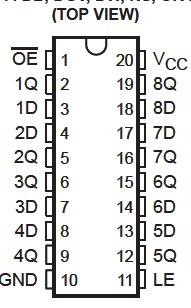
Pinout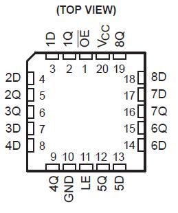
 Specifications
Supply voltage range, VCC . . . . . . . . . . . . . . . . . . . . . . . . . . . . . . . . . −0.5 V to 7 V
Input voltage range, VI (see Note 1) . . . . . . . . . . . . . . . . . . . . . . . . . .−0.5 V to 7 V
Switch I/O voltage range, VIO (see Notes 1 and 2) . . . . . . . .−0.5 V to VCC + 0.5 V
Input clamp current, IIK (VI < 0) . . . . . . . . . . . . . . . . . . . . . . . . . . . . . . . . . .−20 mA
I/O diode current, IIOK (VIO < 0) . . . . . . . . . . . . . . . . . . . . . . . . . . . . . . . . . −50 mA
Switch through current, IT (VIO = 0 to VCC) . . . . . . . . . . . . . . . . . . . . . . . . .±25 mA
Continuous current through VCC or GND . . . . . . . . . . . . . . . . . . . . . . . . . . . ±50 mA
Package thermal impedance, JA (see Note 3): D package . . . . . . . . . . . . . 73°C/W
(see Note 3): DB package . . . . . . . . . . . ..82°C/W
(see Note 3): DGV package . . . . . . . . . . 120°C/W
(see Note 3): NS package . . . . . . . . . . . . ..64°C/W
(see Note 3): PW package . . . . . . . . . . ...108°C/W
(see Note 4): RGY package . . . . . . . . . . . . .39°C/W
Storage temperature range, Tstg . . . . . . . . . . . . . . . . . . . . . . . . . . ..−65°C to 150°C
DescriptionThe SN74LV373A devices are octal transparent D-type latches designed for 2-V to 5.5-V VCC operation.
While the SN74LV373A latch-enable (LE) input is high, the Q outputs follow the data (D) inputs. When LE is taken low, the Q outputs are latched at the logic levels set up at the D inputs.
A buffered output-enable (SN74LV373A OE ) input can be used to place the eight outputs in either a normal logic state (high or low) or the high-impedance state. In the high-impedance state, the outputs neither load nor drive the bus lines significantly. The high-impedance state and increased drive provide the capability to drive bus lines without need for interface or pullup components.
SN74LV373AOE does not affect the internal operations of the latches. Old data can be retained or new data can be entered while the outputs are in the high-impedance state.
To ensure the high-impedance state during power up or power down, SN74LV373A OE should be tied to VCC through a pullup resistor; the minimum value of the resistor is determined by the current-sinking capability of the driver.
The SN54LV373A is characterized for operation over the full military temperature range of 55°C to 125°C. The SN74LV373A is characterized for operation from 40°C to 85°C.

 SN74LV373A Data Sheet


