Pinout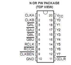 SpecificationsSupply voltage range, VCC. . . . . . . . . . . . . . . . . . . . . . . . . . . .-0.5 V to 7 V
Input voltage range, VI (see Note 1) . . . . . . . . . . . . . . . . . . . .-0.5 V to 7 V
Voltage range applied to any output in the high-impedance
or power-off state, VO(see Note 1) . . . . . . . . . . . . . . . . . . . . .-0.5 V to 7 V
Output voltage range, VO(see Notes 1 and 2) . . . . . . . -0.5 V to Vcc+ 0.5 V
Input clamp current, IIK (VI < 0) . . . . . . . . . . . . . . . . . . . . . . . . . . . ..-20 mA
Output clamp current, IOK (VO< 0) . . . . . . . . . . . . . . . . . . . . . . . . .. .-50 mA
Continuous output current, IO(VO = 0 to VCC) . . . . . . . . . . . . . . . .±35 mA
Continuous current through VCC or GND . . . . . . . . . . . . . . . . . . . . .±70 mA
Package thermal impedance,JA (see Note 3):N package . . . . . . .69/W
PW package . . . . . .83/W
Storage temperature range, Tstg. . . . . . . . . . . . . . . . . . . . . . -65 to 150
Description The SN74LV8154 is a dual 16-bit binary counter with 3-state output registers, designed for 2-V to 5.5-V VCC operation.
This SN74LV8154 16-bit counter (A or B) feeds a 16-bit storage register, and each storage register is further divided into anupper byte and lower byte.The GAL,GAU, GBL, GBU inputs are used to select the byte that needs to be output
at Y0-Y7. CLKA is the clock for A counter, and CLKB is the clock for B counter. RCLK is the clock for the A and
B storage registers. All three clock signals are positive-edge triggered.
A 32-bit counter SN74LV8154 can be realized by connecting CLKA and CLKB together and by connecting RCOA to CLKBEN.
To ensure the high-impedance state during power up or power down, SN74LV8154 GAL, GAU, GBL, and GBU should be tied to VCC through a pullup resistor; the minimum value of the resistor is determined by the current-sinking capability
of the driver.
This device SN74LV8154 is fully specified for partial-power-down applications using Ioff. The Ioff circuitry disables the outputs,
preventing damaging current backflow through the device when it is powered down.

 SN74LV8154 Data Sheet


