Features: ` 1.4-k Pullup Resistors Integrated on All Open-Drain Outputs Eliminate the Need for Discrete Resistors
` ESD Protection Exceeds 2000 V Per MIL-STD-883, Method 3015; Exceeds 200 V Using Machine Model (C = 200 pF, R = 0)
` Designed for the IEEE Std 1284-I (Level 1 Type) and IEEE Std 1284-II (Level 2 Type) Electrical Specifications
` Flow-Through Architecture Optimizes PCB Layout
` Package Options Include Plastic 300-mil Shrink Small-Outline (DL) and Thin-Shrink Small-Outline (DGG) PackagesPinout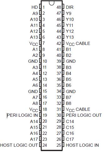 Specifications
Supply voltage range: VCC CABLE . . . . . . . . . . . . . . . . . . . . . . . . . . . . . . . . . . . . . . . . . . 0.5 V to 7 V
VCC . . . . . . . . . . . . . . . . . . . . . . . . . . . . . . . . . . . . . . . . . . . . . . 0.5 V to 4.6 V
Input and output voltage range, VI and VO: Cable side (see Notes 1 and 2) . . . . . . . . . . 2 V to 7 V
Peripheral side (see Note 1) . . . . . 0.5 V to VCC + 0.5 V
Input clamp current, IIK (VI < 0) . . . . . . . . . . . . . . . . . . . . . . . . . . . . . . . . . . . . . . . . . . . . . . . . 20 mA
Output clamp current, IOK (VO < 0) . . . . . . . . . . . . . . . . . . . . . . . . . . . . . . . . . . . . . . . . . . . . . . 50 mA
Continuous output current, IO: Except PERI LOGIC OUT . . . . . . . . . . . . . . . . . . . . . . . . . . . . . . ±50 mA
PERI LOGIC OUT . . . . . . . . . . . . . . . . . . . . . . . . . . . . . . . . . . ±100 mA
Continuous current through each VCC or GND . . . . . . . . . . . . . . . . . . . . . . . . . . . . . . . . . . . . . ±200 mA
Output high sink current, ISK (VO = 5.5 V and VCC CABLE = 3 V) . . . . . . . . . . . . . . . . . . . . . . . . . 65 mA
Package thermal impedance, JA (see Note 3): DGG package . . . . . . . . . . . . . . . . . . . . . . . . . 89°C/W
DL package . . . . . . . . . . . . . . . . . . . . . . . . . . . 94°C/W
Storage temperature range, Tstg . . . . . . . . . . . . . . . . . . . . . . . . . . . . . . . . . . . . . . . . 65°C to 150°C
† Stresses beyond those listed under "absolute maximum ratings" may cause permanent damage to the device. These are stress ratings only, and functional operation of the device at these or any other conditions beyond those indicated under "recommended operating conditions" is not implied. Exposure to absolute-maximum-rated conditions for extended periods may affect device reliability.
NOTES: 1. The input and output voltage ratings may be exceeded if the input and output current ratings are observed.
2. The ac input voltage pulse duration is limited to 40 ns if the amplitude is greater than 0.5 V.
3. The package thermal impedance is calculated in accordance with JESD 51.
DescriptionThe SN74LVC161284 is designed for 3-V to 3.6-V VCC operation. This device provides asynchronous two-way communication between data buses. The control-function implementation minimizes external timing requirements.
This device has eight bidirectional bits; data can flow in the A-to-B direction when DIR is high, and in the B-to-A direction when DIR is low. This device also has five drivers, which drive the cable side, and four receivers. The SN74LVC161284 has one receiver dedicated to the HOST LOGIC line and a driver to drive the PERI LOGIC line.
The SN74LVC161284 output drive mode is determined by the high-drive (HD) control pin. When HD is high, the outputs are in a totem-pole configuration, and in an open-drain configuration when HD is low. This meets the drive requirements as specified in the IEEE Std 1284-I (level 1 type) and IEEE Std 1284-II (level 2 type) parallel peripheral-interface specifications. Except for HOST LOGIC IN and PERI LOGIC OUT, all cable-side pins have a 1.4-kW integrated pullup resistor. The pullup resistor is switched off if the associated output driver is in the low state or if the output voltage is above VCC CABLE. If VCC CABLE is off, PERI LOGIC OUT is set to low.
The device SN74LVC161284 has two supply voltages. VCC is designed for 3-V to 3.6-V operation. VCC CABLE supplies the inputs and output buffers of the cable side only and is designed for 3-V to 3.6-V and for 4.7-V to 5.5-V operation. Even when VCC CABLE is 3 V to 3.6 V, the cable-side I/O pins are 5-V tolerant.
The SN74LVC161284 is characterized for operation from 0°C to 70°C.

 SN74LVC161284 Data Sheet


